
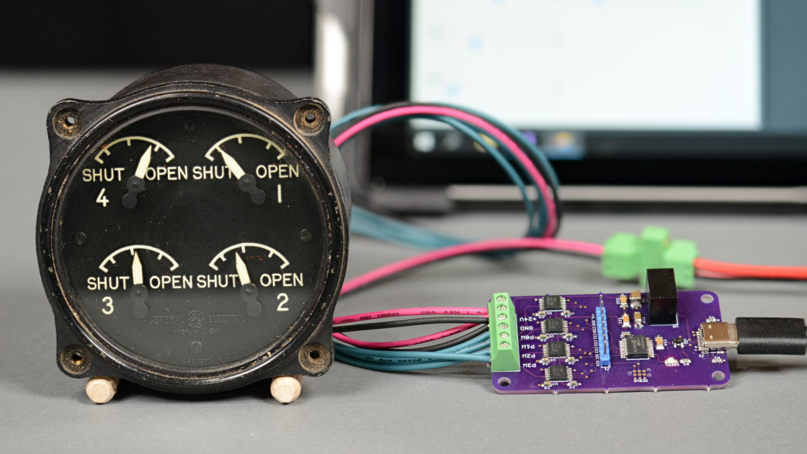
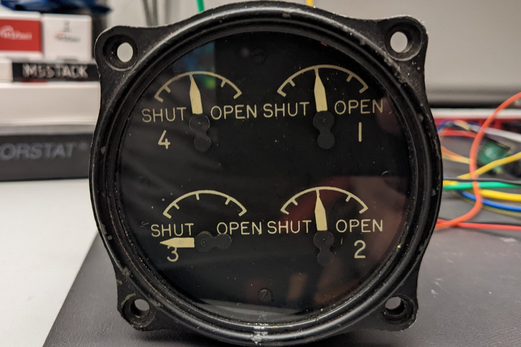
General Electric 8DJ4PBV quad engine cowling indicator with PIC16F1459 and MCP41HV31-502 board to its right. A Microsoft Surface in the background is controlling the indicators via USB.
In this project, I convert a WW2-era engine cowl flaps indicator into a USB peripheral using a Microchip PIC16F1459 microcontroller and four Microchip MCP41HV31-502 digital potentiometers. This project is reminiscent of my USB analog panel meters project but the drive circuitry is significantly less complex. This post starts with a look at the engine cowl indicator, it’s theory of operation, and some ideas to control it using modern electronics. The post then covers the design of the board, the software for the microcontroller, and a Visual Studio C# .NET Windows Forms app for controlling the indicators from a PC.
General Electric DC Selsyn Indicators
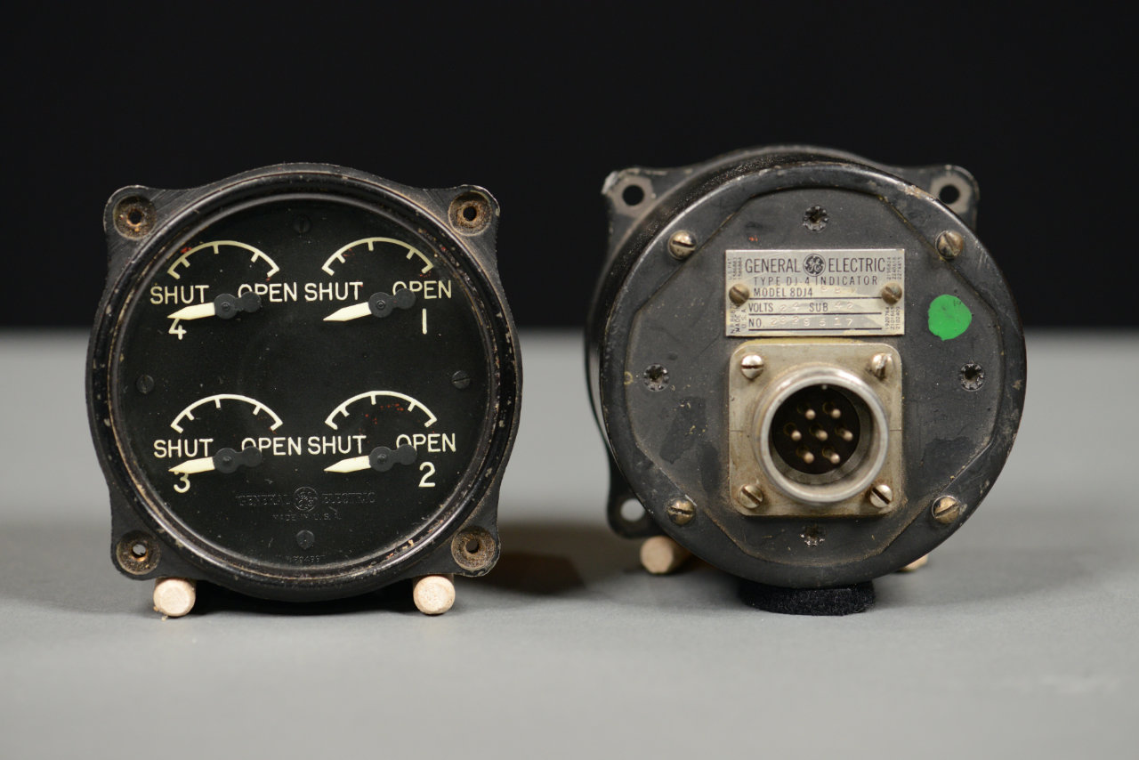
Front and rear view of the General Electric model 8DJ4PBV engine cowl flaps indicator.
This indicator is a General Electric model 8DJ4PBV DC Selsyn indicator. It is one of about 50 different varieties of General Electric DC Selsyn indicators. These indicators were commonly used on US and UK military aircraft employing DC electrical systems during the WWII-era in the 1940s. Their operation manual states these indicators were used to give the pilot a “visual indication of the position of landing wheels, landing flaps, cowl flaps, oil cooler flaps, or similar movable parts of the airplane structure.”
This specific meter is used to indicate the position of the engine cowl flaps on a four-engine aircraft. If you’re wondering what engine cowl flaps are, the Aircraft Owners and Pilots Association has a brief explanation: “Cowl flaps are small doors located in the bottom of the engine cowling that allow for greater cylinder cooling during takeoff and climb. The pilot operates the flaps by opening and closing them via mechanical or electrical controls in the cockpit.”
When a pilot commands the engine cowl flaps to open or close, a mechanical actuator moves the cowl flaps, a transmitter senses the position of the flaps, and this indicator indicates the position of the flaps as sent by the transmitter–if everything is working. If everything is not working, the pilot could detect the failure by the disparity between the controls for the cowl flaps and the indicated position of the cowl flaps. Some possible causes of failure could be that the cowl is stuck open or closed or there’s a defect in the transmitter, indicator, or the wiring between the transmitter and indicator.
Theory of Operation
The theory of operation for these indicators is described in great detail in Army Air Forces publication AN 05-55A-1, Operation and Service Instructions for D-C Selsyn Position Indicators and Transmitters, 20 June 1944, revised 10 June 1945. This document can be rented for $6/month or purchased for $37.82 at https://aircorpslibrary.com. I have excerpted the relevant parts of this document in this post for the purposes of educating others on the operation of these historic indicators.
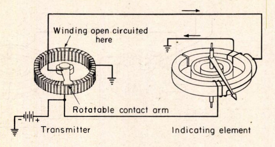
Schematic of a two-wire DC Selsyn system from Operation and Service Instructions for D-C Selsyn Position Indicators and Transmitters. There are four indicating elements in the 8DJ4PBV indicator.
The figure above is a schematic of the two-wire DC Selsyn system from the service and operation manual. This indicator has four two-wire indicating elements that connect to four transmitters, one transmitter per engine cowl flap.
On the left side of the schematic is the transmitter. The transmitter consists of a potentiometer connected across a DC power source with the wiper of the potentiometer connected to the indicating element.
On the right side of the schematic is the indicating element. It consists of two coils of wire wrapped around a ring with a small gap opposite the two coils. The coils are spaced 120 degrees apart and connected across the same DC power source as the potentiometer. The wiper of the potentiometer is connected between the two coils.
Inside the ring is a rotor with a permanent magnet and an indicating needle. The small gap in the ring focuses the magnetic flux in the region between the two coils where the rotor’s magnet is located. The rotor will then rotate toward the vector sum of the magnetic flux generated in the coils.
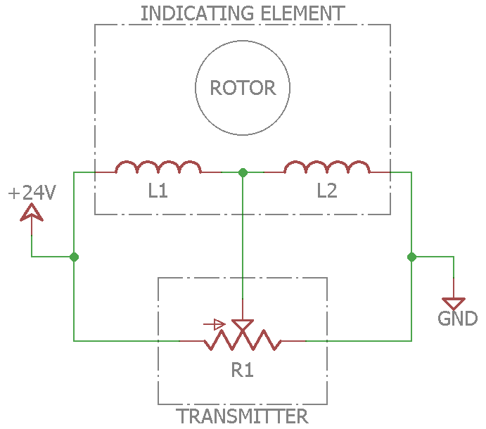
Simplified two-wire DC Selsyn schematic.
The above diagram is a simplified version of the previous schematic drawn using modern CAD symbols. To see how the two-wire DC Selsyn works, consider three different wiper positions of R1. R1 has been split into two discrete resistors with a constant sum of 500 Ohms for the purposes of analysis in the figure below.
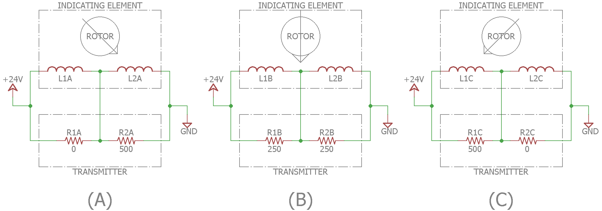
Three different positions of the wiper on R1. R1 has been split into R1 and R2 on this schematic.
With the potentiometer at the extreme left as shown in (A), the current in the first coil will be zero and thus the magnetic field generated in that coil will also be zero. The permanent magnet rotor will then swing toward the second energized coil where current is flowing and magnetic flux is being generated.
With the potentiometer halfway through its rotation as shown in (B), the current in the first coil and the current in the second coil will be identical and thus the magnetic flux generated in both coils will be equal too. The rotor will be evenly attracted to both coils and swing to the middle.
With the potentiometer at the other extreme as shown in (C), the current in the second coil will be zero and thus the magnetic field generated in that coil will also be zero. The rotor will now be attracted to the first coil and swing to the left.
In Practice

Internal connections of indicator model 8DJ4PBV41.
The figure above shows the internal connections of the four indicator elements in this model of indicator. Note that there’s a resistor in series with the middle of the two coils and the wiper of the transmitter’s potentiometer that is not present in the theory of operation schematics. Each coil has an internal resistance of about 1800 Ohms and the resistor has a resistance of about 300 Ohms. This model is spec’ed for 24 V DC operation.
The other interesting point to make about this diagram is that each indicating element is rotated with respect to the others. The needles are then mounted to the rotors such that they swing from about 45 degrees left of top center through top center to about 45 degrees right of top center. In other words, the needles are aligned to their scales on the face plate regardless of the actual orientation of the coils and rotors under the face plate.
In this meter, there’s also a small spring on each rotor that pulls the needles out of the minimum and maximum scale region when the meter has no DC power.
Initial Testing

Connection diagram for an 8DJ4PBV indicator with four Mallory M-500-P potentiometers used as transmitters.
Once I had an indicator in hand, it was time to test it. Luckily, the service and operations manual contains a connection diagram, a portion of which is shown above. The connection diagram illustrates how to connect the indicator to a 24 V DC power source and four Mallory M-500-P 500 Ω, 4 Watt potentiometers. The manual also lists the part number of the connector required to connect to the meter.
I did not have the mating connector nor did I have a 500 Ω, 4 Watt potentiometer. Time to improvise! I used leads with insulated alligator clips to connect to the connector pins and a small 10 kΩ potentiometer.
This indicator is broken. With 24 V DC power applied and no connections to the centers of the coils, all four indicators should be pointed at mid-scale. Indicator number 3 is a dud.
I selected indicator 3 and turned power on. It kind of worked. The needle moved back and forth as I turned the potentiometer but the needle jumped around a lot and positioning wasn’t repeatable. Turns out indicator 3 was broken. I moved the alligator clips to one of the other indicators and operation was perfect. Even with a small 10 kΩ, 1/4 Watt potentiometer instead of a massive 500 Ω, 5W potentiometer.
Going Back to eBay
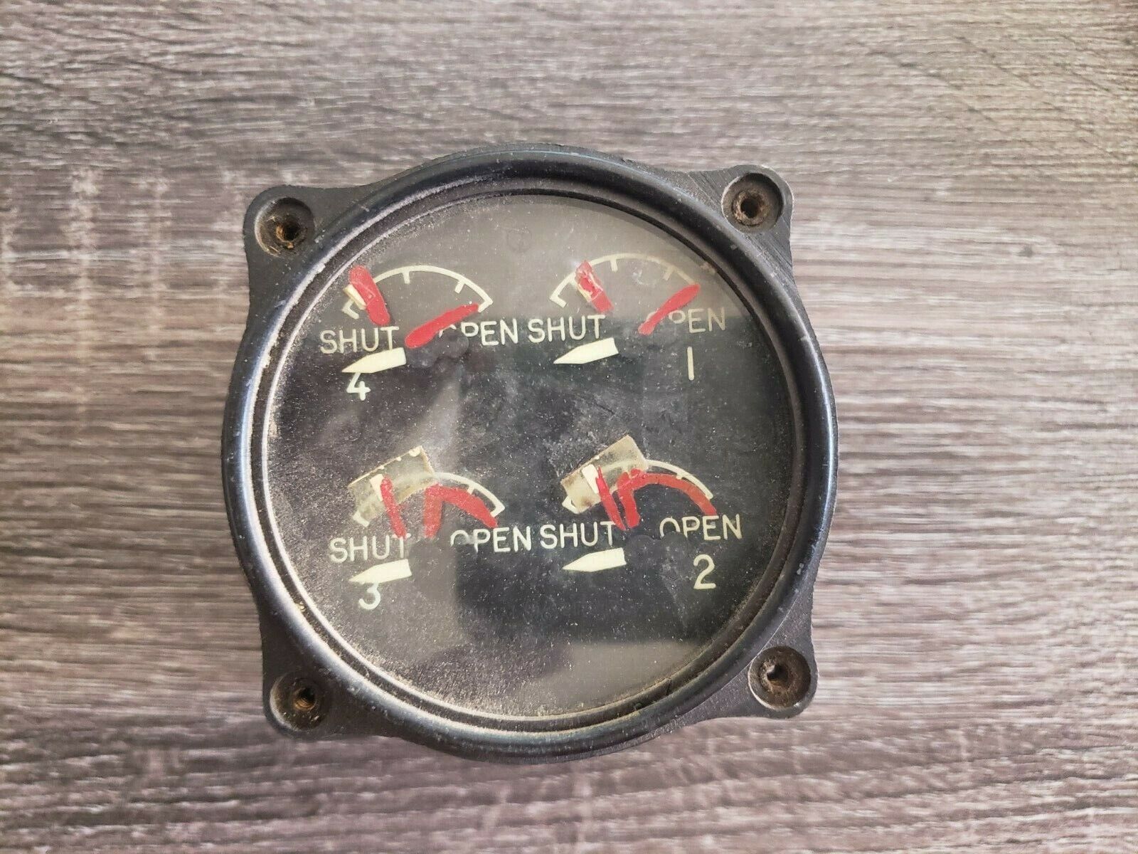
I found another 8DJ4PBV indicator that looks like its seen better days.
I went back to eBay and found the above meter. That’s the listing image. It definitely looks like it has seen better days. It was about $10 so figured I’d give it a try. I also found and ordered a new-old-stock Amphenol MS3106A16S-1S connector to connect to the meter.
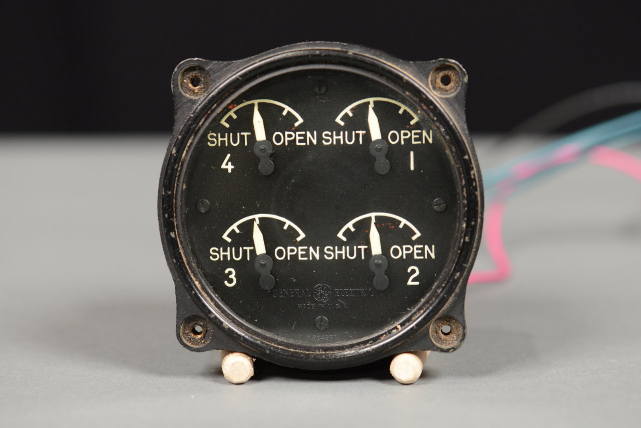
The 2nd eBay indicator after a thorough scrubbing. Notice how all four needles point to about mid-scale? Much better results than the first indicator.
When it arrived, I cleaned it up and tried it out. Success! When powered up, all four indicators moved to their half-scale positions. I connected my 10 kΩ potentiometer’s wiper to each dial’s connector pin in succession and verified the needles moved smoothly from one side of the scale to the other as I turned the potentiometer’s shaft. The other really cool bit is using a 10 kΩ potentiometer instead of a 500 Ω potentiometer seems to work well but cuts the current consumption significantly. This is an important consideration for the next section of this post.
Selecting a Digital Potentiometer
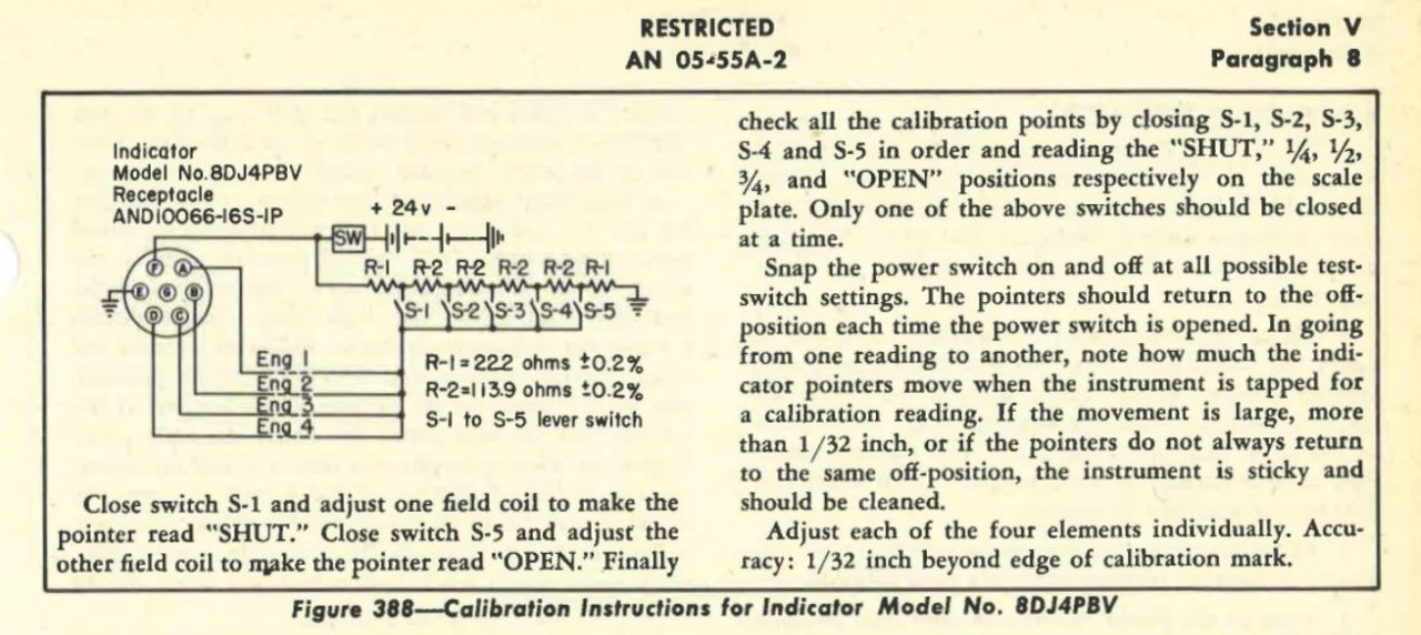
8DJ4PBV calibration instructions.
The last interesting tidbit in the service and operation manual for this meter is the calibration instructions shown in the image above. See that group of resistors and switches used as part of the test jig? What does it look very, very similar too?
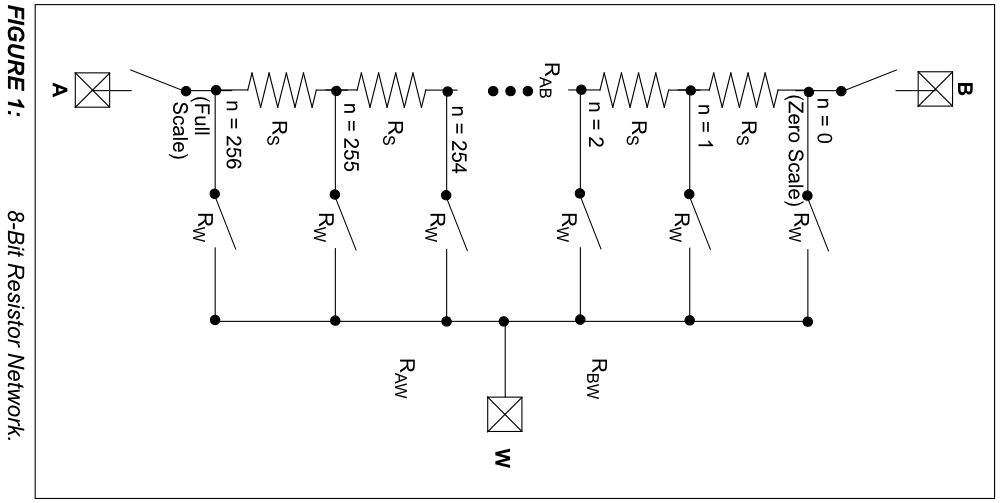
Microchip AN1080 Resistor Network
Well, it’s practically identical to the resistor and switch network in a digital potentiometer! Would it be possible to use a digital potentiometer to control the position of the needles on this indicator? That would boil down to two concerns: 1) are there digital potentiometers that can handle 24 Volts? and 2) are there digital potentiometers that can handle whatever currents the indicators require?
Digital potentiometers have three key specification regarding the extremes they can tolerate. The first is the maximum terminal voltage range. This is the voltage across terminals A and B in the resistor network figure shown above. The second is the maximum current into or out of the A, B, and W terminals. The last is the maximum package power dissipation.
The terminal voltage for our application is simply our DC supply voltage of 24 Volts. To specify the required terminal currents for our application requires some calculations. Calculating the A, B, and wiper current with the wiper at either of the two extremes and in the middle will be sufficient in our application.
Left Extreme Current Calculation

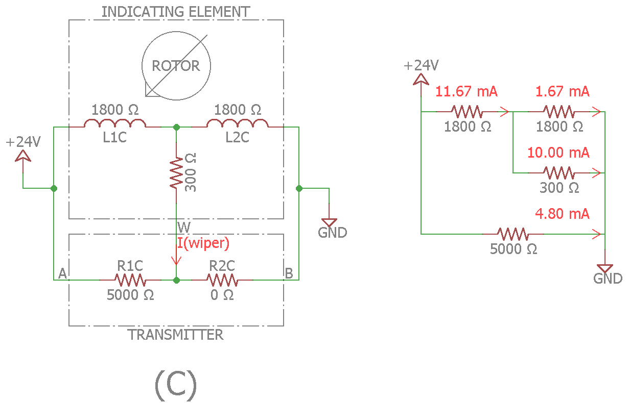
On the left, the resistances of the circuit components with the wiper moved to the extreme left. On the right, a simplified version of the same drawing annotated with the current calculations.
The schematic above shows the equivalent circuit of the indicator using a 5 kΩ potentiometer as a transmitter and with the potentiometer positioned at its extreme left toward the 24 V DC supply voltage. In this case, the wiper is sourcing 10 mA of current to the indicator.
There’s also a current of 24 V / 5 kΩ = 4.8 mA from terminal A to the terminal B from the 5k resistance. This results in the following currents through the terminals:
- Into terminal A: 10 mA + 4.8 mA = 14.8 mA
- Out of the wiper terminal: 10 mA
- Out of terminal B: 4.8 mA
The maximum current through any terminal in this case is 14.8 mA.
Center Current Calculation

On the left, the resistances of the circuit components with the wiper centered. On the right, a simplified version of the same drawing annotated with the current calculations.
The schematic above shows the equivalent circuit of the indicator using a 5 kΩ potentiometer as a transmitter and with the potentiometer positioned halfway between the 24 V DC supply and the DC supply ground. In this case, no current is flowing into or out of the wiper because the voltages at either side of the indicator’s internal 300 Ω resister are the same. Of course, the resistors won’t be perfectly matched in real life so a small current will still flow into or out of the wiper terminal but they’ll be small compared to when the wiper is at one extreme or the other.
Including the current from the 5 kΩ terminal resistance results in the following currents through the terminals:
- Into terminal A: 4.8 mA
- Out of the wiper terminal: 0 mA
- Out of terminal B: 4.8 mA
The maximum current through any terminal in this case is 4.8 mA.
Right Extreme Current Calculation
On the left, the resistances of the circuit components with the wiper moved to the extreme right. On the right, a simplified version of the same drawing annotated with the current calculations.
The schematic above shows the equivalent circuit of the indicator using a 5 kΩ potentiometer as a transmitter and with the potentiometer positioned at its extreme right toward the DC supply ground. In this case, the wiper is sinking 10 mA of current from the indicator.
Including the current from the 5 kΩ terminal resistance results in the following currents through the terminals:
- Into terminal A: 4.8 mA
- Into the wiper terminal: 10 mA
- Out of terminal B: 14.8 mA
The maximum current through any terminal in this case is 14.8 mA.
Package Power Dissipation
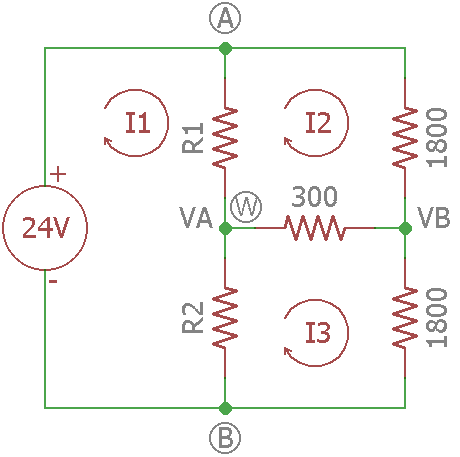
Circuit used for mesh analysis and power dissipation calculations.
Calculating the maximum package power dissipation for the design is a bit tougher. The power dissipation is dependent on the current through the resistors in the resistor network which will vary based on the selected resistance tap.
Let’s make some graphs to illustrate the change in power dissipation as the resistance is adjusted. We’ll use the figure above and mesh analysis to solve for the power dissipation in the potentiometer as a function of R1. First use mesh analysis to come up with a system of simultaneous equations for the circuit:
- R1*(I1-I2)+R2*(I1-I3)=V
- R1*(I2-I1)+1800*I2+300*(I2-I3)=0
- R2*(I3-I1)+300*(I3-I2)+1800*I3=0
- R1+R2 = 5000
- V = 24
I cheated and plugged these into Wolfram Alpha to solve for I1, I2, and I3:
- I1 = (V (R1 (R2 + 2100) + 300 (7 R2 + 14400)))/(3600 (R1 (R2 + 1200) + 1200 R2))
- I2 = (V (R1 (R2 + 2100) + 300 R2))/(3600 (R1 (R2 + 1200) + 1200 R2))
- I3 = (V (R1 (R2 + 300) + 2100 R2))/(3600 (R1 (R2 + 1200) + 1200 R2))
From there, I created an Octave script to vary R1 from 0 to 5000 and calculate the power dissipated in R1 and R2 and the total power dissipation:
% R1*(A1-A2)+R2*(A1-A3)=V,
% R1*(A2-A1)+1800*A2+300*(A2-A3)=0,
% R2*(A3-A1)+300*(A3-A2)+1800*A3=0,
% solve for A1,A2,A3

% inputs
V = 24;
R1 = 0:1:5000;
R2 = 5000 - R1;

% currents in loops
I1 = (V.*(R1.*(R2 + 2100) + 300.*(7.*R2 + 14400)))./(3600.*(R1.*(R2 + 1200) + 1200.*R2));
I2 = (V.*(R1.*(R2 + 2100) + 300.*R2))./(3600.*(R1.*(R2 + 1200) + 1200.*R2));
I3 = (V.*(R1.*(R2 + 300) + 2100.*R2))./(3600.*(R1.*(R2 + 1200) + 1200.*R2));

% wiper voltage and coil center voltage
VA=R2.*(I1-I3);
VB=1800.*I3;

% voltage across R1 inside pot
VR1 = R1 .* (I1-I2);

% voltage across R2 inside pot
VR2 = R2 .* (I1-I3);

% this should be 24 V
VPOT = VR1 + VR2;

% power dissipated in pot A resistor
PAW = R1.*(I2-I1).^2;

% power dissipated in pot B resistor
PWB = R2.*(I3-I1).^2;

% total power dissipation in pot
PD = PAW + PWB;
PAW is the power dissipated in R1, PWB is the power dissipated in R2. These are calculated as P = (I^2)(R) where R is either R1 or R2 and I is the current through the respective resistor using the terms from the mesh analysis.
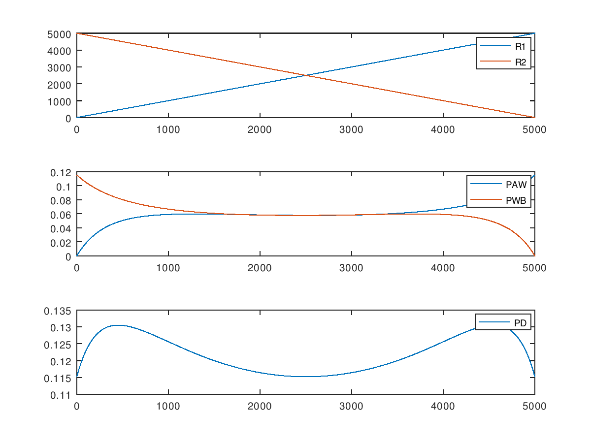
Top graph is R1 and R2 vs R1. All in Ohms. Middle graph is power dissipated in R1 and power dissipated in R2 versus R1. Power in Watts, resistance in Ohms. Finally, the bottom graph is the total power dissipation in both resistors versus R1. Again, power in Watts, resistance in Ohms.
From looking at the graph, I can see the maximum power dissipation occurs at R1 = 452 Ohms and is 130.5 mW. We need to select a potentiometer in a package with a maximum power dissipation rating of at least 130.5 mW.
Final Requirements
Based on the calculated terminal and wiper currents, my final requirements for a digital potentiometer were:
- Single-ended terminal voltage >> 24 Volts.
- Terminal and wiper current >> 14.8 mA.
- Maximum package power dissipation >> 130.5 mW.
Selected Part: Microchip MCP41HV31-502E/ST

Top 2/3rd’s of the first page of the Microchip MCP41HVX1 datasheet.
At this point, I searched manufacturers’ datasheets for a high-voltage digital potentiometer with sufficient terminal and wiper current capacity to meet the above requirements. The Microchip MCP41HV31-502 and MCP41HV51-502 parts both meet my requirements. An excerpt from the first page of the data sheet is shown above.
They both support a maximum single-ended terminal voltage of 36 Volts which is greater than my requirement of 24 Volts. The 5 kΩ version supports terminal and wiper currents of 25 mA which is greater than my requirement of 14.8 mA. According to the Absolute Maximum Ratings section of the datasheet, the maximum package power dissipation for the device in the TSSOP-14 package is 1000 mW which greatly exceeds my maximum anticipated power dissipation of 130.5 mW.
The only difference between the two parts is that one is 7 bits with 128 resistance steps while the other is 8 bits with 256 resistance steps. I did some prototyping with the 8-bit part and decided that 7 bits / 128 steps was sufficient for my application.
Building a Test Board
The next step was to build a small test board to ensure I understood how these parts worked and test how they would interact with the indicator. This test board contains only one digital potentiometer and, as a result, can only control one of the four dials on the indicator.
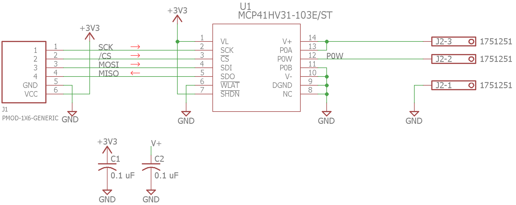
Test board schematic.
Shown above is the schematic for the single channel test board. A six-pin 0.1″ header is used to supply power to the pot’s digital logic and provide access to its bidirectional SPI bus. A 3.5 mm, three-position screw terminal strip supplies 24 V DC to the digital pot’s A and B terminals and provides access to the wiper terminal for connecting to the indicator. Two small decoupling caps are placed across the logic and 24 V supplies.
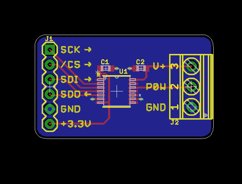
Test board layout.
The completed board layout is shown above. The final board measured 1.2 x 0.7 inches and cost $4.20 to have manufactured at OSH Park.
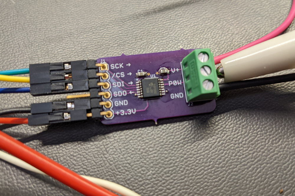
My fully populated MCP41HV51-502E/ST test board.
When the board arrived, I stuffed the board with a few connectors, capacitors, and a MCP41HV51-502E/ST 256-step digital potentiometer chip. I attached the SPI bus to a microcontroller dev board and the screw terminals to one of the four dials on the indicator. I powered everything up and it worked great with the 256-step part. After a few more tests, I decided the lower-cost (and still available) 128-step part would work just as well as the 256-step part. Time to design a board with a built-in microcontroller to control all four dials on the indicator.
Expanding to Four Channels
After building a test board and demonstrating that the MCP41HV31-502 digital potentiometer could be used to control one of the dials, it was time to build a board to control all four dials simultaneously. The board also needed its own USB microcontroller and 24 VDC power supply.
Microcontroller Selection
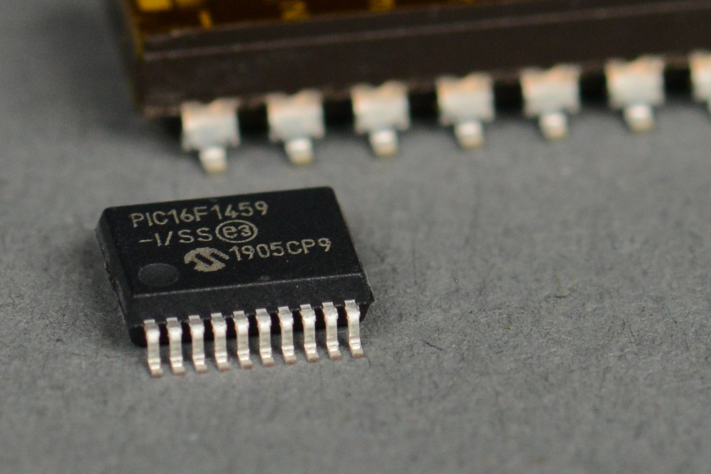
PIC16F1459 in a TSSOP-20 package next to an eight position SMD switch.
For this project, I’m going to use the Microchip PIC16F1459 8-bit USB microcontroller. I’ve used this microcontroller before so I’m familiar with the required support circuitry and USB software. An 8-bit microcontroller is fine for this application because it only needs to implement the USB stack, listen for USB OUT reports, and control the digital potentiometers over a SPI bus in response to the USB OUT reports.
Power Supply
The board’s power input will be the same voltage as the meters, 24 V DC. The microcontroller and digital potentiometers require 5 V DC. I’m using a CUI VX7805-500 three-terminal linear regulator replacement to power the micro and pots. It requires 10 µF and 0.1 µF caps on the input and 22 µF and 0.1 µF caps on the output as described in the datasheet. The VX7805 is a switching DC/DC converter. Compared to a linear regulator like the LM7805, the VX7805 has a much wider input voltage range of 6.5 to 36 Volts, a higher efficiency of 90%, and runs cool to the touch.
Schematic
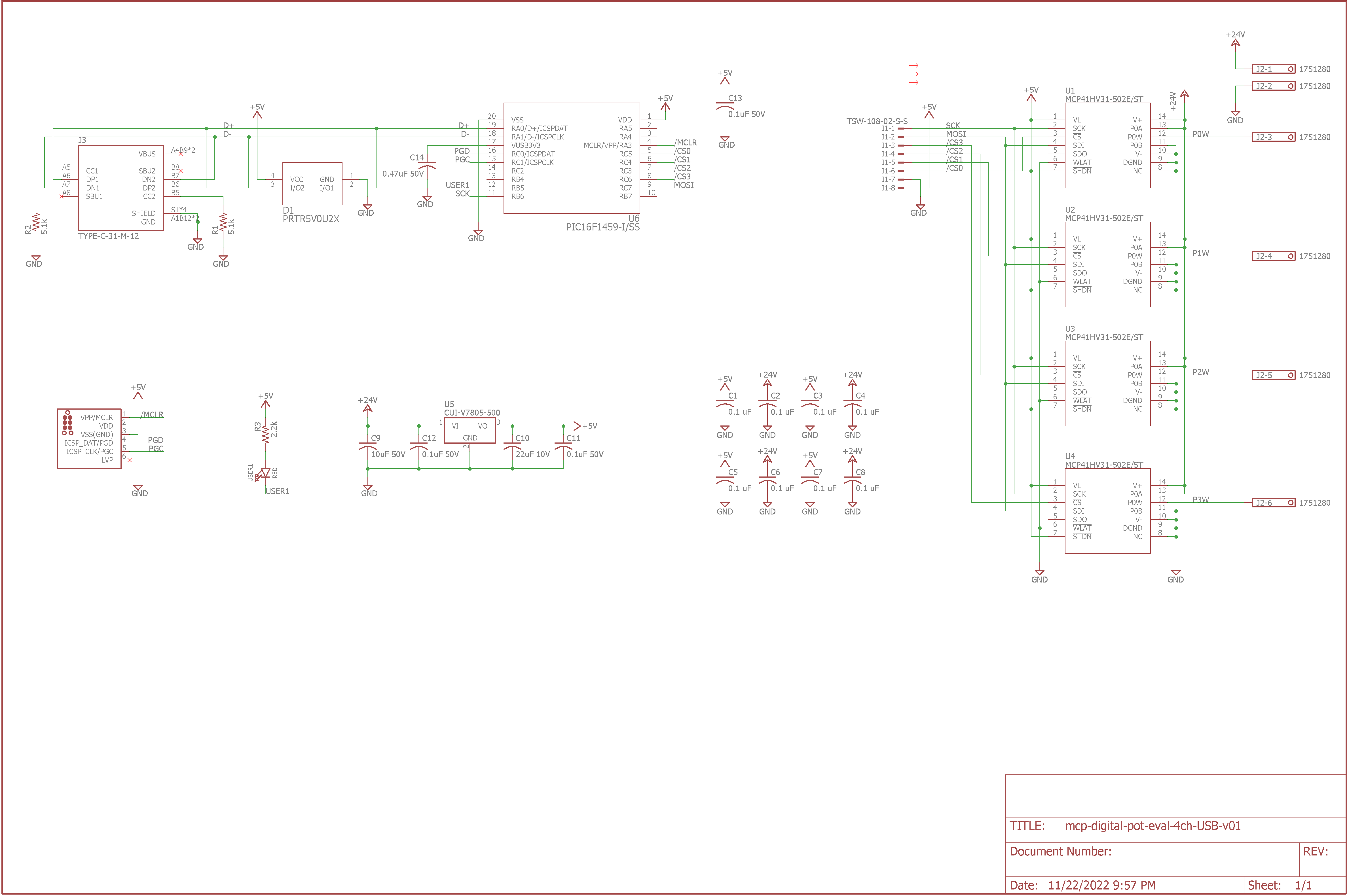
Four channel USB digital potentiometer board schematic.
With the selection of the power supply, microcontroller, and digital potentiometers done, it was time to draw the schematic. This is a USB self-powered design meaning the board is powered by its own power supply rather than a USB bus-powered design that is powered by the USB host.
Technically, there should be a net from the USB bus’s VBUS pin to the micro so the micro can place its D+/D- pins in a high-impedance state until the USB host drives VBUS high. From the PIC16F1459 datasheet: “In order to meet compliance specifications, the USB module (and the D+ or D- internal pull-ups) should not be enabled until the host actively drives VBUS high.” I’m not going to seek USB certification for this board so I’m not going to worry about it.
For more detailed information on using the PIC16F1459 and the support circuitry I’ve included in this design, I recommend reading my Updates to the Annoying CAPS LOCK Warning Buzzer post.
Board Layout

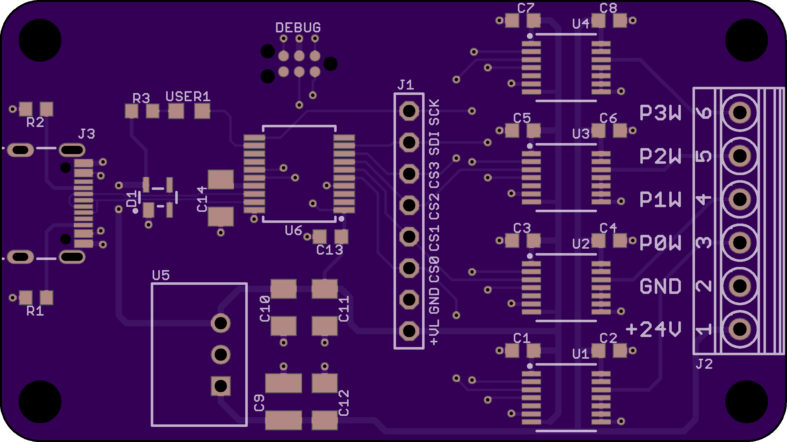
Four channel USB digital potentiometer board schematic.
The completed board layout is shown above. The USB and microcontroller stuff is on the left. The digital pots and connections to the indicators and power suppy are on the right. I placed 0.1″ header in the center of the board for debugging the SPI bus. If the microcontroller section of the board is not stuffed, an off-board microcontroller could be connected to the header and used instead of the on-board PIC16F1459.
Board Preview
Render of the top of the four channel USB digital potentiometer board.
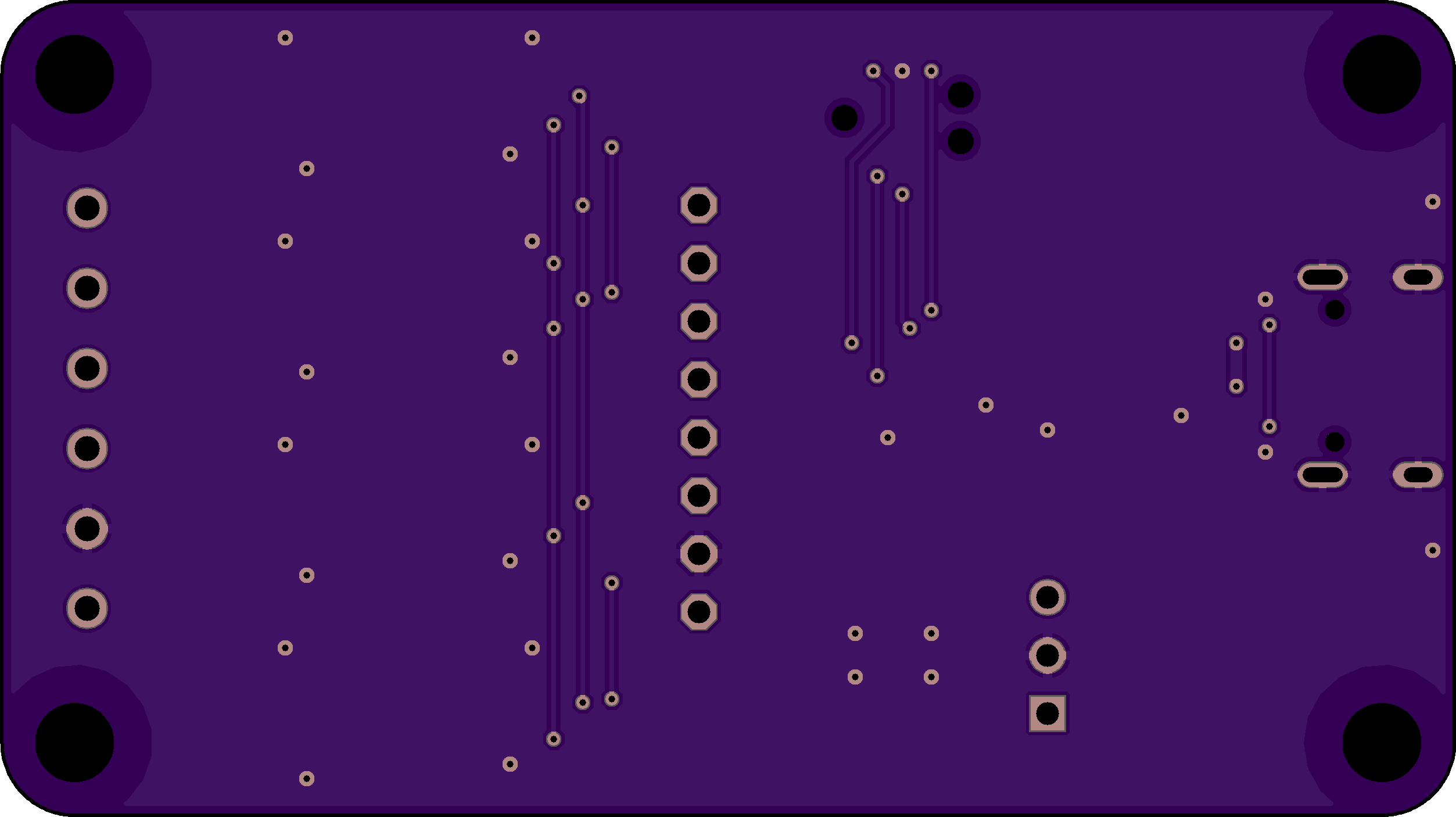
Render of the bottom of the four channel USB digital potentiometer board.
Once the board layout was complete, I uploaded the Gerbers to OSH Park and examined the board renders for any mistakes. After one or two revisions to get the silkscreen correct, I ordered the boards.
Fabricated Boards
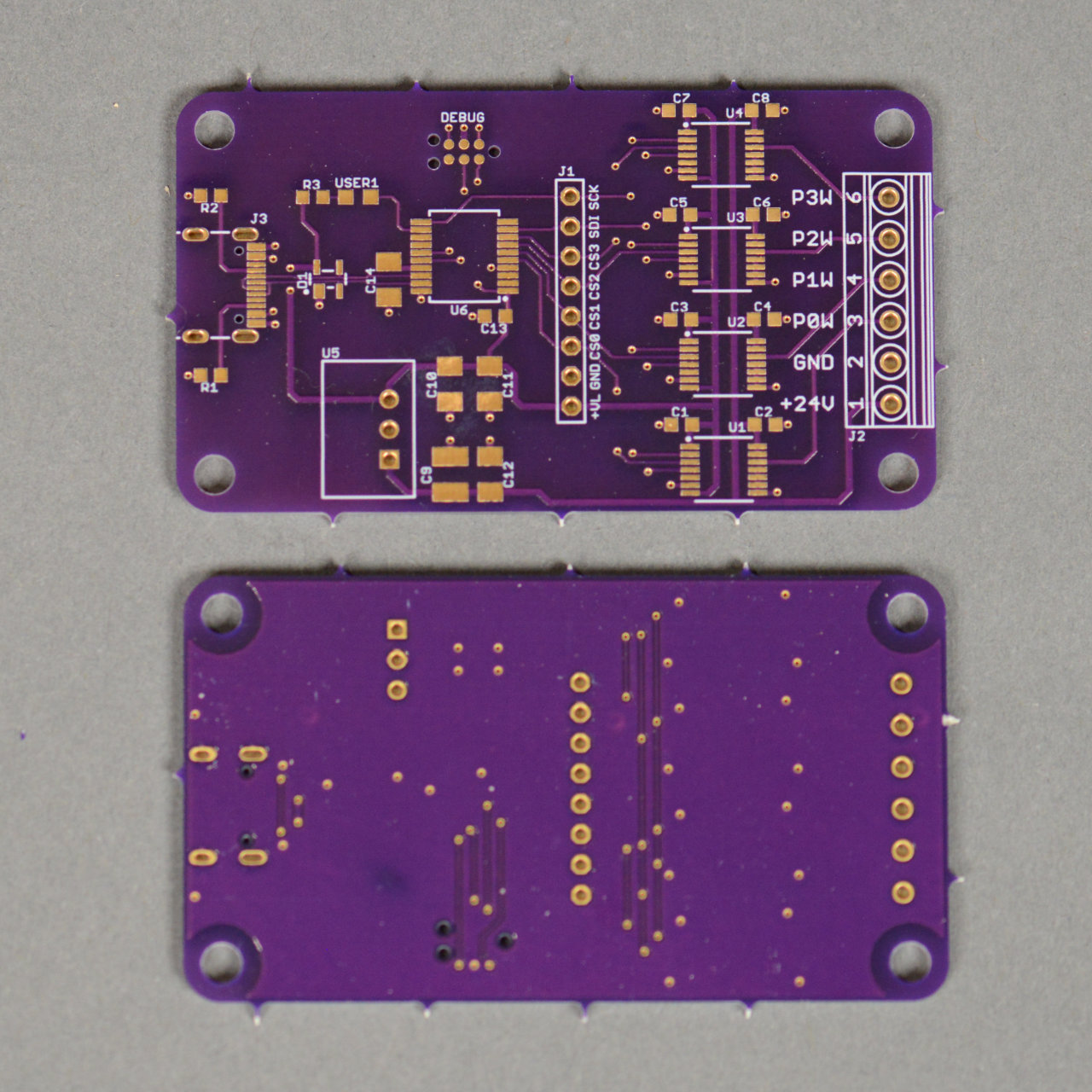
The front and back of the fabbed boards.
About two weeks later I received the boards.
Board Assembly
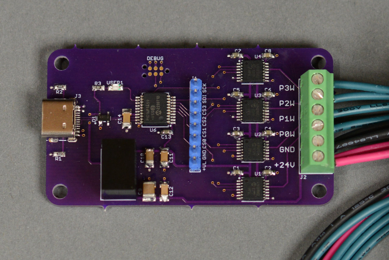
The completed and assembled board. The board features a USB 2.0 Type C connector, a PIC16F1459, four MCP41HV31 digital potentiometers, and a screw terminal strip to connect to power and the indicator.
The completely assembled board is shown above. I assembled and tested the board in stages though. First up was to stuff the power supply, USB components, LED, and microcontroller. After stuffing thsee parts, I programmed an existing PIC16F1459 USB software design into the micro and verified the USB and micro worked.
With USB and the micro working, I disconnected the board and soldered a single MCP41HV31 digital pot to the board. I then modified the software to control the digital pot. Once I was happy that everything was working properly, I soldered the remaining digital pots to the board.
I expanded the software to drive four digital pots and did a bit more testing. Everything worked so it was time to connect to the meter. I built the board up in stages mostly due to the silicon and parts shortage. I did not want to solder all the chips to the board just to find out the board didn’t work and have to scramble to find additional components.
Connecting to the Meter
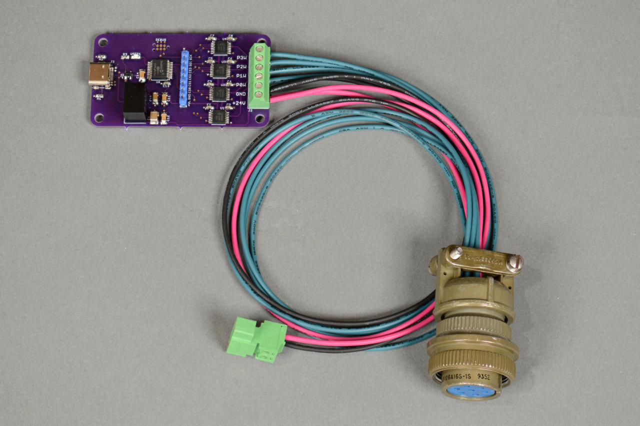
The completed USB controller board with green Phoenix power connector and drab olive Amphenol indicator connector.
The connection to the meter is made using an Amphenol MS3106A16S-1S connector. This is a solder connector. I’m getting better at soldering solder cup terminals in tight spaces like on this connector but I’m by no means great at it yet. Two tricks I’ve learned:
- Don’t use PVC-insulated wire. PVC insulation melts. Instead use XLPE (like in the image above) or PTFE (Teflon) insulated wire. The insulation on these wires is much more heat resistant than cheap PVC insulation.
- Heat shrink covers all sins. If you’re stuck using PVC-insulated wire and the insulation melts, slip some heatshrink down over the mess and call it good. Heatshrink is often used in aerospace applications even with PTFE-insulated wire anyway to protect the wire and prevent shorts around the solder joint.
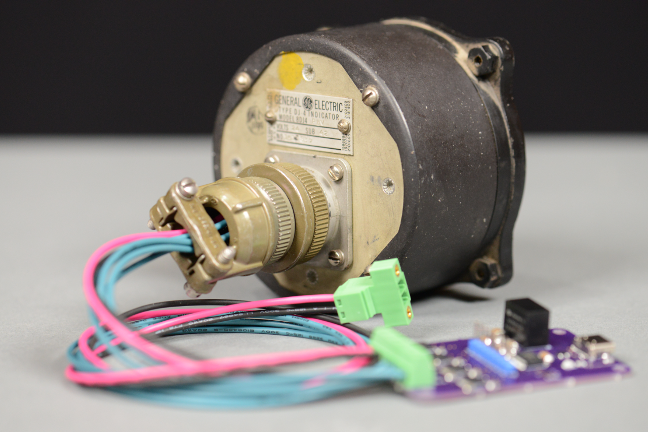
USB controller board connected to indicator with the large Amphenol connector.
The board connected to the indicator. After working with these indicators, my estimate is half the weight of an aircraft is connectors and wire harnesses. These things are just bulky and heavy.
PIC16 Embedded Software
The PIC16 software for this project builds on the Microchip Library for Applications USB HID custom device example and the past work I’ve done using this library. The most recent incarnation of this work was the USB DIP switch and I used a cleaned up version of that code as a starting point for this project.
USB Report Descriptor
A vendor-defined custom HID peripheral needs a USB report descriptor. I’m using a report descriptor that is compatible with the USB analog meters project so that I can reuse the C# .NET app for this project.
The first report ID is a USB OUT report from the USB host to the USB device. It allows the USB host to set all four digital potentiometer levels at once. It’s four bytes, one byte per meter. Only values from 0 to 127 are valid.
The second report ID is a USB OUT report from the USB host to the USB device. It allows the USB host to set a single digital potentiometer at a time. It’s two bytes. The first byte is the digital potentiometer to set from 0 to 3 and the second byte is the level from to 127.
Unlike the USB analog meters project, this board has no PWM hardware so I did not include the third report ID from that project. The complete USB report descriptor is shown below.
// Class specific descriptor - HID
// 4 bytes in to set all indicators at once, 4 values from 0 to 0x7F
// 2 bytes in to set a single meter at a time, 1 value from 0 to 3, 1 value from 0 to 0x7F
const struct{uint8_t report[HID_RPT01_SIZE];}hid_rpt01={
{

        0x06, 0x00, 0xFF,  // Usage Page (Vendor Defined 0xFF00)
        0x09, 0x01,        // Usage (0x01)
        0xA1, 0x01,        // Collection (Application)

        0x85, 0x01,        //   Report ID (1)
        0x95, 0x04,        //   Report Count (4)
        0x75, 0x08,        //   Report Size (8)
        0x26, 0xFF, 0x00,  //   Logical Maximum (255)
        0x15, 0x00,        //   Logical Minimum (0)
        0x09, 0x01,        //   Usage (0x01)
        0x91, 0x02,        //   Output (Data,Var,Abs,No Wrap,Linear,Preferred State,No Null Position,Non-volatile)

        0x85, 0x02,        //   Report ID (2)
        0x95, 0x02,        //   Report Count (2)
        0x75, 0x08,        //   Report Size (8)
        0x26, 0xFF, 0x00,  //   Logical Maximum (255)
        0x15, 0x00,        //   Logical Minimum (0)
        0x09, 0x01,        //   Usage (0x01)
        0x91, 0x02,        //   Output (Data,Var,Abs,No Wrap,Linear,Preferred State,No Null Position)

        0xC0,              // End Collection

        // 38 bytes
}};
USB Callbacks
The USB callbacks are located in the APP_DeviceCustomHIDTasks function:
void APP_DeviceCustomHIDTasks()
{
    /* If the USB device isn't configured yet, we can't really do anything
     * else since we don't have a host to talk to.  So jump back to the
     * top of the while loop. */
    if( USBGetDeviceState() < CONFIGURED_STATE )
    {
        return;
    }

    /* If we are currently suspended, then we need to see if we need to
     * issue a remote wakeup.  In either case, we shouldn't process any
     * keyboard commands since we aren't currently communicating to the host
     * thus just continue back to the start of the while loop. */
    if( USBIsDeviceSuspended()== true )
    {
        return;
    }

    //Check if we have received an OUT data packet from the host
    if(HIDRxHandleBusy(USBOutHandle) == false)
    {
        // switch report ID
         switch (ReceivedDataBuffer[0]) {
            case 0x01:
                irqMetersUpdateFlags = 0x0f;
                irqMetersLevels[0] = ReceivedDataBuffer[1];
                irqMetersLevels[1] = ReceivedDataBuffer[2];
                irqMetersLevels[2] = ReceivedDataBuffer[3];
                irqMetersLevels[3] = ReceivedDataBuffer[4];
                break;
            case 0x02:
                if ((ReceivedDataBuffer[1] >= 0) && (ReceivedDataBuffer[1] <= 3)) {
                    irqMetersUpdateFlags |= (1 << ReceivedDataBuffer[1]);
                    irqMetersLevels[ReceivedDataBuffer[1]] = ReceivedDataBuffer[2];
                }
                break;
        }

        //Re-arm the OUT endpoint, so we can receive the next OUT data packet
        //that the host may try to send us.
        USBOutHandle = HIDRxPacket(CUSTOM_DEVICE_HID_EP, (uint8_t*)&ReceivedDataBuffer[0], 64);
    }
}
This code sets some flags and values telling the main loop code to update the indicators. Since this code is called from the main loop and is not running at interrupt time (despite the variable names!), sending the values over SPI to the digital potentiometers could be done here instead. The code is this way mostly because it was ported from the EFM8UB1 where this code was running at interrupt time.
Main Loop
The main loop code receives the flags and values from the APP_DeviceCustomHIDTasks function. The flags tell the main loop code which meters need to be updated and the values are the values to send to the digital potentiometer. For each flag that is set, the microcontroller clears the flag and bit bangs out the specified value.
        // update meters if needed
        mainMetersUpdateFlags = irqMetersUpdateFlags;
        for (i = 0; i < 4; i++) {
            mainMetersLevels[i] = irqMetersLevels[i];
        }
        irqMetersUpdateFlags = 0;

        if (mainMetersUpdateFlags & 1) {
            pot_Write (0, mainMetersLevels[0]);
        }

        if (mainMetersUpdateFlags & 2) {
            pot_Write (1, mainMetersLevels[1]);
        }

        if (mainMetersUpdateFlags & 4) {
            pot_Write (2, mainMetersLevels[2]);
        }

        if (mainMetersUpdateFlags & 8) {
            pot_Write (3, mainMetersLevels[3]);
        }
There’s some other code in the main loop that blinks the LED according to the USB state.
Bit Banged SPI
Since the indicator update rate and data rates are so slow, I bit banged the SPI bus rather than using the PIC16F1459’s SPI.
void pot_Write (uint8_t select, uint8_t level)
{
    uint8_t hi, lo, d, i;

    // set chip select low
    if (select == 0) {
        CS0n = 0;
    } else if (select == 1) {
        CS1n = 0;
    } else if (select == 2) {
        CS2n = 0;
    } else if (select == 3) {
        CS3n = 0;
    }

    hi = 0;
    lo = level & 0x7F;

    d = hi;
    for (i = 0; i < 8; i++) {
        SDO = (d & 0x80) ? 1 : 0;
        d = d << 1;
        SCK = 1;
        SCK = 0;
    }

    d = lo;
    for (i = 0; i < 8; i++) {
        SDO = (d & 0x80) ? 1 : 0;
        d = d << 1;
        SCK = 1;
        SCK = 0;
    }

    // all chip selects high
    CS0n = 1;
    CS1n = 1;
    CS2n = 1;
    CS3n = 1;
}
The pot_Write function takes a pot number from 0 to 3 and a value from 0 to 127 then writes the value to the selected pot.
C# .NET Windows Forms App
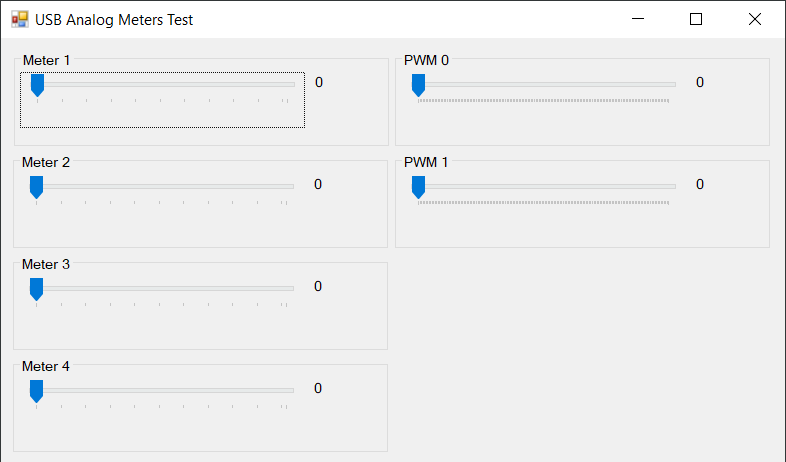
The Visual Studio 2019 C# .NET Windows Forms app for controlling the indicators.
This project reuses the C# .NET Windows Forms app from part two of the USB analog meters project. The only significant difference to the code is the USB VID and PID were updated for the values I selected for this hardware and the scroll bar update scales were changed:
private void trackBar1_ValueChanged(object sender, EventArgs e)
{
    // get trackbar value
    int v = trackBar1.Value;

    // compute value to display in GUI from 0 to 100%
    int display = (int)(100.0 * (float)v / 255.0);

    // compute value to send to hardware
    // 235 for SO-45 meter in enclosure
    // 238 for extremely large switchboard meter
    // 127 for engine cowling indicator
    int send = (int)(127.0 * (float)v / 255.0);

    // update label in GUI
    label1.Text = display.ToString();

    // send data out USB to hardware
    var outData = _device.CreateReport();
    outData.ReportId = 0x02;
    outData.Data[0] = 0;
    outData.Data[1] = (byte)send;
    _device.WriteReport(outData);
}
Moving each of the meter sliders will change the level displayed on its corresponding engine cowl dial. The PWM section is not used in this project.
The Completed Project
The video above is a quick demonstration of the indicator in use. The indicator is connected to the USB controller board and the USB controller board is connected to my Surface. The .NET Forms app is running and superimposed over the video. As I slide the sliders in the app, the corresponding dial moves on the indicator.
Next Steps
Since the indicator is an inductive device, I need to bodge some flyback diodes from each of the digital pot wipers to 24 V DC and ground. I also have an Army-Navy (AN) system selsyn indicator that I’ve built a board to control. The currents are much higher and the drive circuitry is significantly more complex. It will be the topic of a future blog post.
Some comments after the post was published suggested running the design from the USB 5 Volt VBUS supply instead of a separate 24 Volt power supply. While it is true that the indicators are ratiometric and it shouldn’t matter what the supply voltage is, the dials do not reach their full-scale open position with a supply voltage of less than about 18 Volts. My theory is that the reduced currents at lower voltages do not generate enough flux to overcome the loading of the springs that snap the dials to the off-scale loss-of-power position.
Some other comments suggested using PWM outputs or a DAC and an op amp to generate the control signals for the dials. This is definitely possible but was not the route I chose to follow for this design. An op amp can easily achieve an output of 24 V with a drive of ±10 mA.
Design Files
The board design, PIC source code, and C# source code for this project are available on Github in my usb-ww2-engine-cowling repository.