
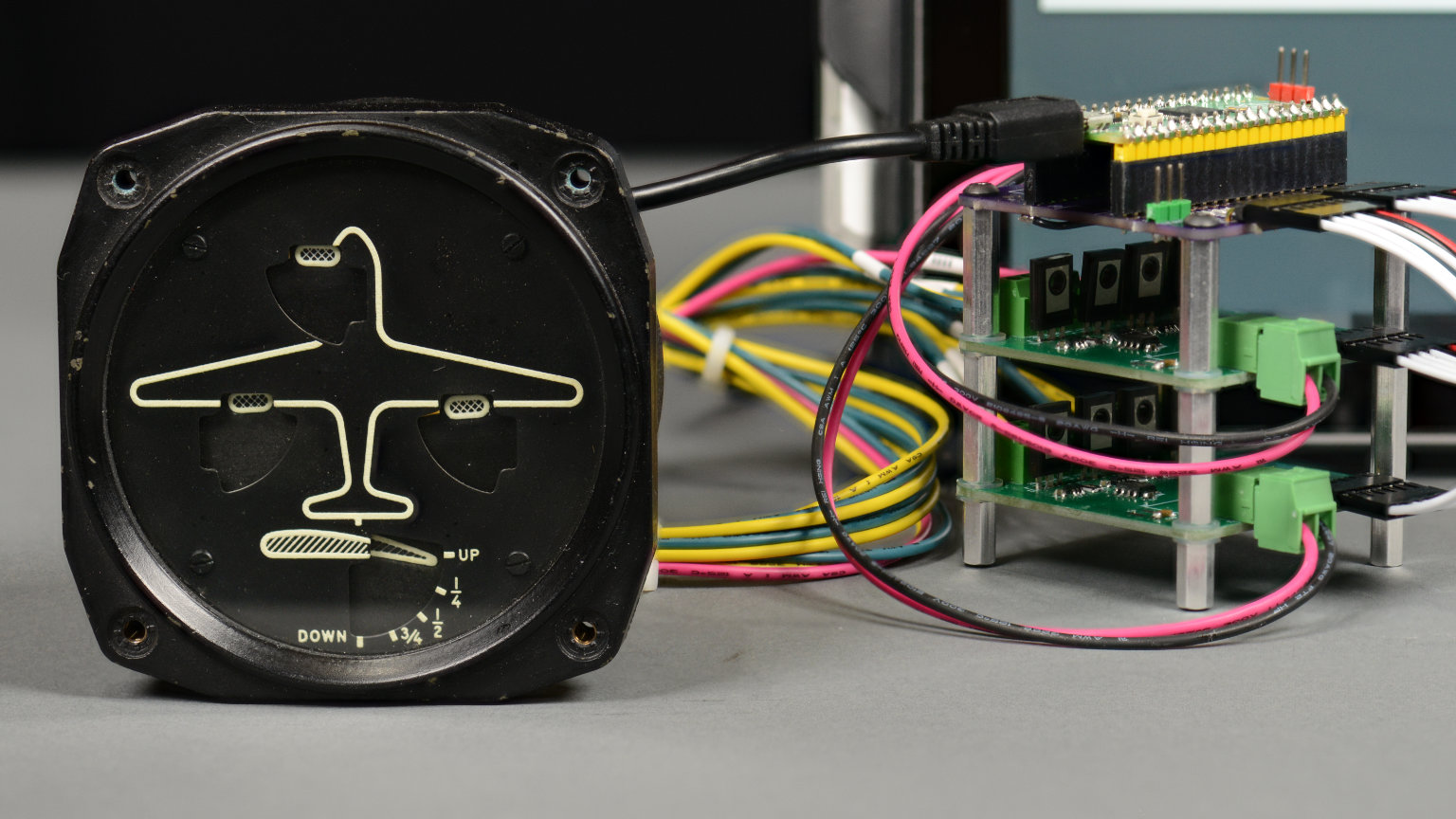
The landing gear and flaps indicator, control board stack, and C# .NET Windows Forms app running on the Surface in the background. Everything set for smooth and level flight!
In this project, I convert a WW2-era landing gear and flaps indicator into a USB peripheral using a Raspberry Pi Pico development board and eight channels of programmable current sources. This project is similar to my WW2-era engine cowl flaps indicator project but the gear and flaps indicator requires a different control strategy.
This post starts with a look at the gear and flaps indicator, its theory of operation including its differences from the engine cowl flaps indicator, and some ideas to control it with modern electronics. The post then covers the design of the boards, the software for the Pico dev board, and a Visual Studio C# .NET Windows Forms app for controlling the indicators from a PC.
General Electric DC Selsyn Army-Navy (AN) System Indicators

The front and back of the indicator.
This indicator is a General Electric model 8DJ17AAW DC Selsyn indicator. It is one of about 50 different varieties of General Electric DC Selsyn indicators. These indicators were commonly used on US and UK military aircraft employing DC electrical systems during the WWII-era in the 1940s. Their operation manual states these indicators were used to give the pilot a “visual indication of the position of landing wheels, landing flaps, cowl flaps, oil cooler flaps, or similar movable parts of the airplane structure.”
This specific meter is used to indicate the position of the landing gear on an aircraft with nose and wing gear, whether the landing gear are locked in place, and the position of the flaps that can be extended from the trailing edges of the wings. The flaps are used during take offs and landing to produce more lift at slower speeds. The flaps are then raised during normal flight to reduce drag and increase efficiency at higher speeds.
Fail Safe Mechanisms
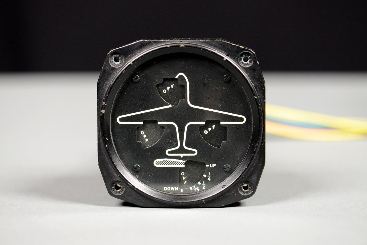
When the indicator has no power, all four dials display the text OFF.
If you look closely at the landing gear and flaps indicators in the photo above, you’ll note that each dial indicates “off” when the indicator is powered down. This is a fail safe mechanism to keep pilots from relying on inaccurate or incomplete data should one or more dials or the entire indicator fail or lose power.
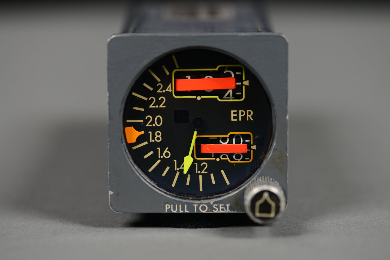
This late 1970’s or early 1980’s engine pressure ratio indicator has two orange flags to indicate the instrument has lost power or has detected an electrical or mechanical malfunction.
This practice continues to this day but the failure state is usually indicated with a fluorescent orange flag covering part of the indicator or with a fluorescent orange flag displaying the word OFF. The flag is displayed upon loss of power or when the instrument senses an electrical or mechanical malfunction.
The Landing Gear Indicators
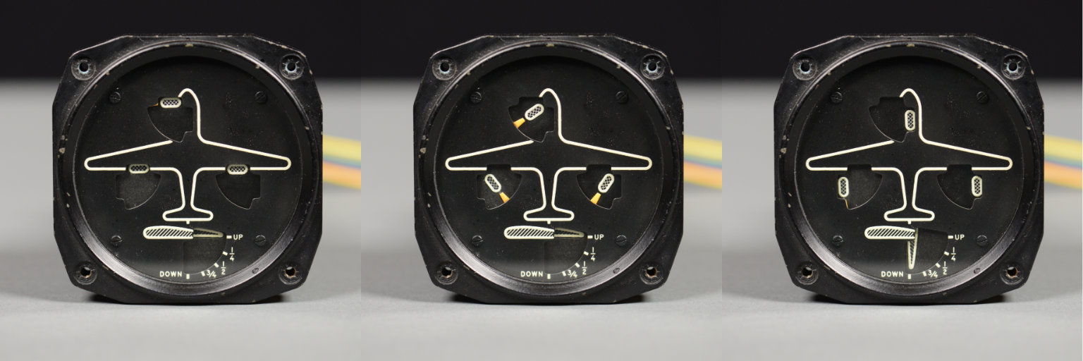
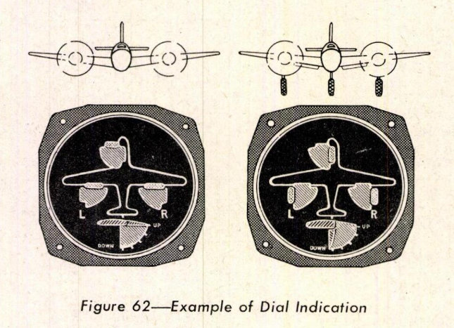
Three photos of the landing gear in various states. The left photo shows the landing gear up and locked. The middle photo shows the landing gear between up and down. The right photo shows the landing gear down and locked.
The photos above show three possible states of the landing gear. In the leftmost photo, the landing gear is up and locked. In the middle photo, the landing gear is unlocked and between the up and down positions. In the rightmost photo, the landing gear is down and locked. The flaps are also down in the rightmost photo.
The presence of the yellow stripe on the landing gear dials indicate the landing gear is somewhere between up and down and is not locked in either position. If the pilot has lowered the gear and expects the landing gear to be down and locked for a landing, the presence of one or more yellow stripes indicates a bad situation.
If you have access to the manual, it’s no longer ambiguous what is up and what is down for the nose gear.
Also, looking at the nose gear dial, it’s a little ambiguous but the nose gear is up and locked when the wheel is horizontal and the nose gear is down and locked when the wheel is vertical. Some versions of this indicator have the word UP stenciled near the nose gear’s horizontal position to eliminate the ambiguity.
In the figure above from the service manual for the indicator, all the gear are up and locked in the left image and the flaps are retracted. All the gear are down and locked in the right image and the flaps are extended.
The Flaps Indicator
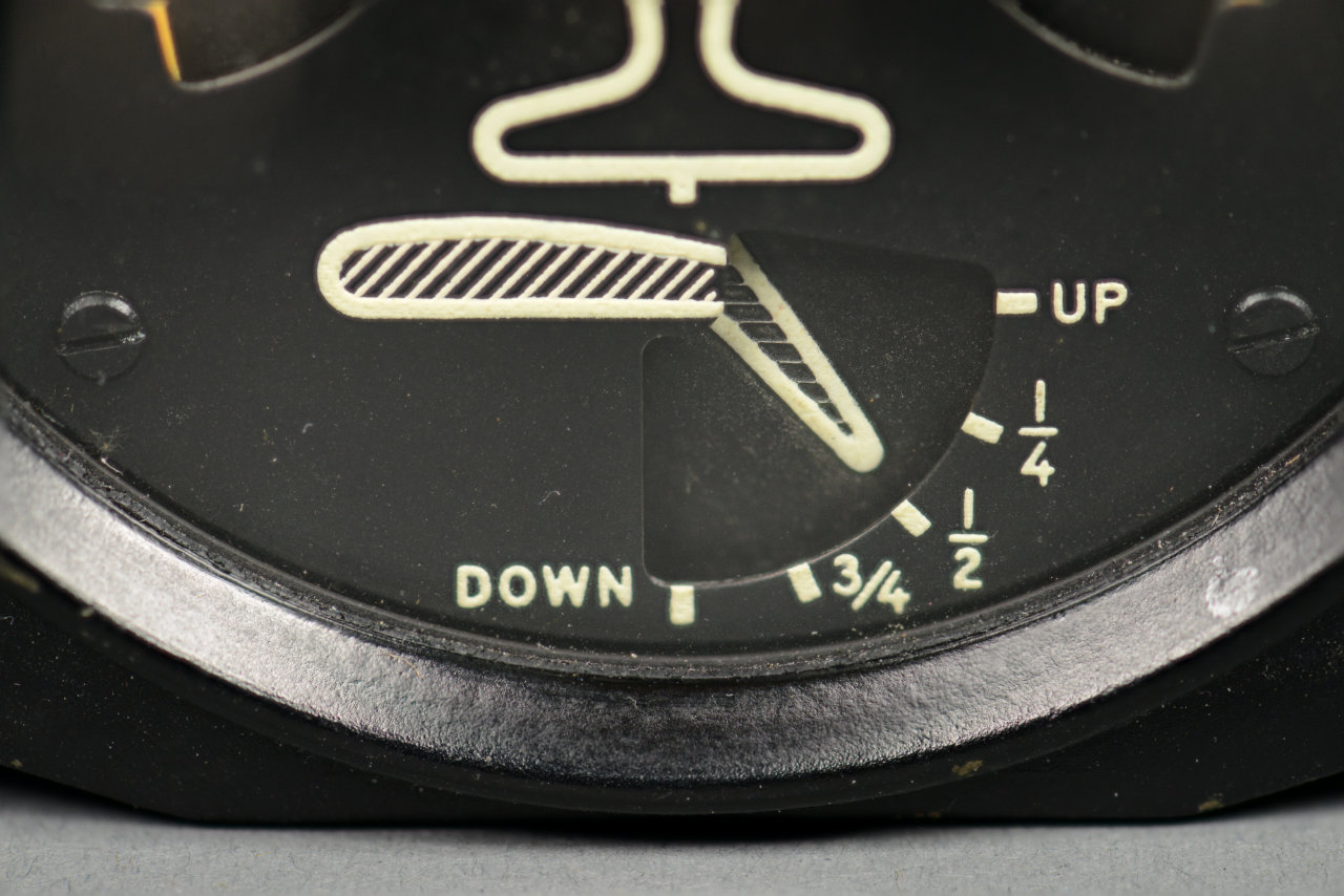
The flaps indicator at about 50%.
The flaps indicator is shown above. The flaps indicator indicates to what extent the flaps are deployed. It consists of a graphical representation of a wing of an aircraft. The leading edge of the wing is on the left and the trailing edge of the wing including the flaps is on the right. The flaps can be up, down, or any position in between. In the photo above, the flaps are extended about 50%.
There’s only one flaps indicator despite aircraft usually having two wings and two sets of flaps. In practice, this means either the flaps were mechanically linked and connected to a single transmitter or two transmitters were connected in parallel to display the average position of both flaps.
The Gear and Flaps Position Transmitter
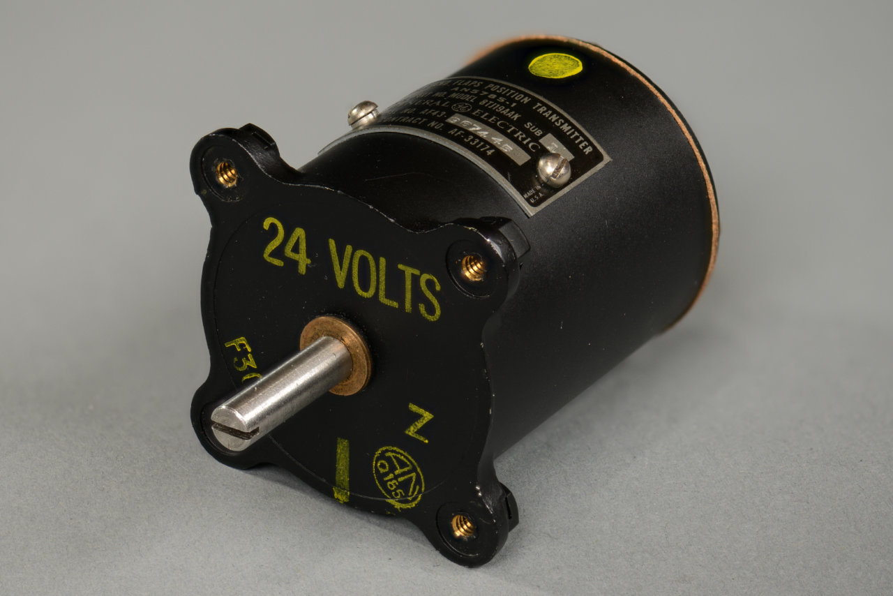
8TJ19AAK landing gear and flaps transmitter.
The photo above shows a model 8TJ19AAK gear and flaps position transmitter. Four of these transmitters are used with this indicator. There’s one transmitter for each set of landing gear and one transmitter (or two transmitters wired in parallel) for the flaps. In addition, a separate pair of limit switches are wired into each of the landing gear’s transmitters to indicate if the gear is locked up or down.
Theory of Operation
The theory of operation for these indicators is described in great detail in Army Air Forces publication AN 05-55A-1, Operation and Service Instructions for D-C Selsyn Position Indicators and Transmitters, 20 June 1944, revised 10 June 1945. This document can be rented for $6/month or purchased for $37.82 at https://aircorpslibrary.com. I have excerpted the relevant parts of this document in this post for the purposes of educating others on the operation of these historic indicators.
Schematic and Mechanical Operation
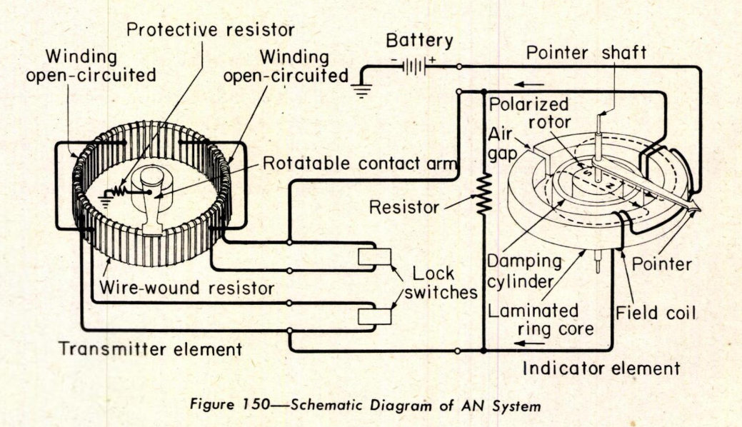
AN system schematic with transmitter, indicator, and lock switches.
Whereas the engine cowl flaps indicator was a two-wire DC Selsyn indicator, the landing gear and flaps indicator is an Army-Navy (AN) system DC Selsyn indicator. The figure above is a schematic of an AN system DC Selsyn from the service and operation manual.
On the left side of the schematic is the transmitter. Ignoring the lock switches and parallel resistance at the back of the transmitter coil, the transmitter basically consists of a potentiometer connected across two wires from the indicator element’s coils with the wiper of the potentiometer connected to the power supply ground through a current limiting resistor. As the wiper is moved from one extreme to the other, the current in one of the indicator’s coils increases while the current in the opposite coil decreases.
In operation, the wiper moves along the portion of the resistance coil between the two innermost lock switch leads. This permits the landing gear dials to move between the up and down positions but maintains sufficient resistance between the indicator’s coils and ground that the dial cannot spin all the way to a locked position.
When a lock switch is closed, it causes a short across a portion of the winding effectively moving the wiper closer to the lead from the indicator coil, reducing the resistance, increasing the current, causing the dial to spin the rest of the way to the locked position, and hiding the yellow warning flag.
On the right side of the schematic is the indicating element. It consists of two coils of wire wrapped around a ring with a small gap opposite the two coils. The coils are spaced 120 degrees apart with a wire connecting the inside ends of each coil together. The DC power supply is connected to this wire between the two coils. Two wires from the outside ends of each coil connect to the transmitter.
Inside the ring is a rotor with a permanent magnet and an indicating dial. The small gap in the ring focuses the magnetic flux in the region between the two coils where the rotor’s magnet is located. The rotor will then rotate toward the vector sum of the magnetic flux generated in the coils.
Simplified Schematic
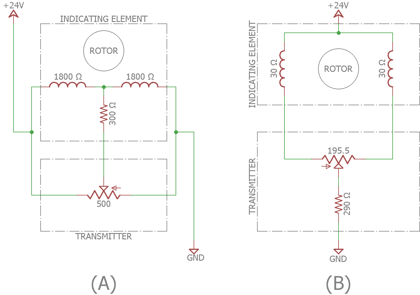
(A) is a simplified schematic of the two-wire Selsyn system. (B) is a simplified schematic of the AN Selsyn system. Eagle PCB does not support components at angles so pay no attention to the relative angles and positions of the coils and rotors.
The above diagram shows simplified schematics drawn using modern CAD symbols for both the two-wire and AN systems. On the left side of the figure is a simplified schematic of a two-wire indicator and transmitter as used in the engine cowl flaps indicator. On the right side of the figure is a simplified schematic of an AN system indicator and transmitter as used in this gear and flaps indicator.
Both circuits vary the currents in the two coils surrounding the rotor based on the position of a wiper on a resistance coil. As the wiper is moved in one direction, the current in one coil increases and the current in the opposite coil decreases. The changes in currents are reversed when the wiper is moved in the opposite direction.
Each dial in a 24 V AN system uses about 2 W so placing the current limiting resistors in the transmitters inside the wheel wells and wings saves about 8 W of heat from entering the cockpit. Another important consideration regarding the placement of the current limiting resistors is that if you naively connect the indicator to 24 V without a transmitter and without any current limiting, the coils inside the meter will overheat and self-destruct.
Electrical Operation and Circuit Analysis
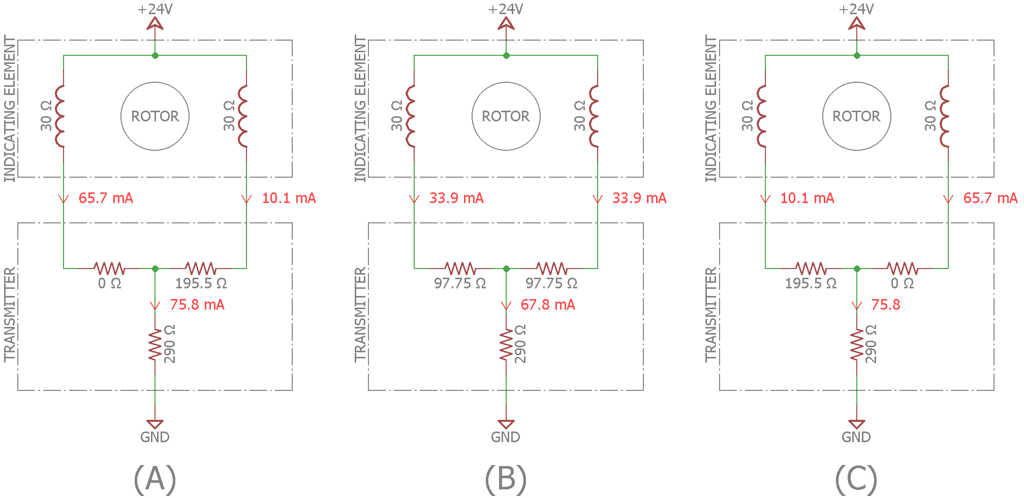
Circuits showing three different positions of the potentiometer wiper
To see how the AN system DC Selsyn works, consider three different positions of the 195.5 Ω potentiometer’s wiper as shown in the three circuits above. The 195.5 Ω potentiometer has been split into two fixed resistors with the values (R) and (195.5 – R) where R is 0 in (A), 195.5 / 2 in (B), and 195.5 in (C).
With the potentiometer at the extreme left as shown in (A), the current in the first coil will be much higher than the current in the second coil. The permanent magnet rotor will then spin toward the first energized coil where the current and magnetic flux are highest.
With the potentiometer halfway through its rotation as shown in (B), the current in the first coil and the current in the second coil will be identical and thus the magnetic flux generated in both coils will be equal too. The rotor will be evenly attracted to both coils and spin to the middle.
With the potentiometer at the extreme right as shown in (C), the current in the second coil will be much higher than the current in the first coil. The permanent magnet rotor will then spin toward the second energized coil where the current and magnetic flux are highest.
The currents in the AN DC Selsyn system are about five times higher than the currents in the two-wire DC Selsyn system. These currents exceed the capabilities of most common digital potentiometers so a different control strategy will be required for computer control of this indicator.
Initial Testing
Connections
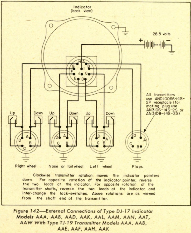
External connections of the 8DJ17AAW indicator.
Once I had a transmitter and indicator in hand, it was time to test them. Luckily, the service and operations manual contains a connection diagram, a portion of which is shown above. The connection diagram illustrates how to connect the indicator to a 24 V DC power source and four transmitters and three sets of lock switches. The manual also lists the part numbers of the connectors required to connect to the indicator and transmitters.
Test Setup
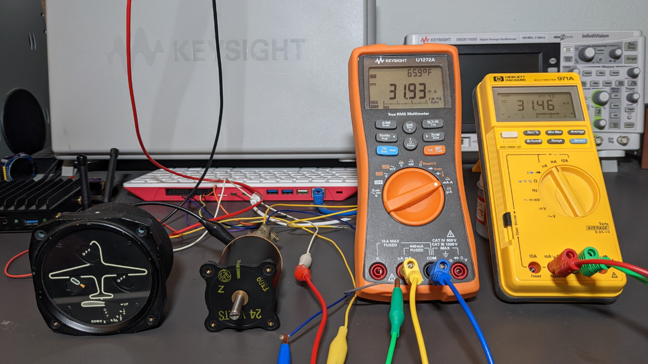
Indicator, transmitter, and two DMMs set to make current measurements.
The photo above shows the test setup. The indicator is on the left, the transmitter is in the middle, and two digital multimeters are on the right. The transmitter is connected to the left landing gear dial according to the connection diagram.
The left DMM is connected in series between the indicator’s (C) pin and the transmitter’s (A) pin and measures the current through the first of the two coils in the left landing gear dial. The right DMM is connected in series between the indicator’s (D) pin and the transmitter’s (D) pin and measures the current through the second of the two coils in the left landing gear dial. The test setup is powered by a programmable bench supply set to 24 V and a current limit of 80 mA.
Test Measurements
Using this test setup, I measured the currents in each leg of the circuit with the landing gear down and locked, the landing gear halfway between up and down, and the landing gear up and locked. These measurements and the currents calculated in the previous section are documented in the table below.
| Landing Gear Position | I(CtoA) Measured | I(DtoD) Measured | I(CtoA) Calculated | I(DtoD) Calculated |
|---|---|---|---|---|
| Down and Locked | 67.01 mA | 7.70 mA | 65.7 mA | 10.1 mA |
| Centered | 31.65 mA | 31.75 mA | 33.9 mA | 33.9 mA |
| Up and Locked | 9.17 mA | 64.90 mA | 10.1 mA | 65.7 mA |
The measured currents are very close to the calculated currents. Referring to the service and operation manual, the acceptable tolerances on the system’s resistance values are quite high and these currents are certainly within the tolerances.
One question I had was if the indicator dial would work with a sum of currents lower than 75 mA. I set the bench supply to a current limit of 50 mA and turned the transmitter shaft back and forth. The indicator dial worked just as well with a total current limit of 50 mA.
I repeated the test with an overall limit of 35 mA. The landing gear dial wouldn’t quite reach the down and locked position with a limit of 35 mA. My design goal will be to use 50 mA currents for controlling the indicator dials.
Power Dissipation

Thermal image of the transmitter in operation.
According to the service manual, the transmitter dissipates about 2 W. The thermal image above shows that this dissipation warms up the transmitter a bit compared to its surroundings.
Design and Component Selection
The dials on the indicator could be driven using PWM or programmable current sinks. In both cases, the current through each of the indicator’s dials’ coils needs to be limited to a maximum of about 50 mA. If PWM is used, current limiting resistors are required to limit the current. This is similar to the 290 Ω current limiting resistor in the transmitter. If programmable current sinks are used, the current is limited by the design of the current sink. I used programmable current sinks for this project.
PWM + Current Limiting Resistors
Example PWM driver schematic.
The schematic above shows two channels of PWM used to control a single dial on the indicator. R1 and R2 control the maximum currents through the dial’s coils. The duty cycle of the PWM waveforms controls the time each coil is energized and thus the average current through the coils. The inductance of the coils and the inertia of the rotor effectively average the PWM current.
The only critical components in this schematic are R1 and R2 which are sized to meet the design goal of a 50 mA maximum current and protect the dial’s coils from excessive current. Since 5 V / 100 Ω is 50 mA, let’s start with 100 Ω as a first approximation to the needed resistance. Since the meter coils have a resistance of 30 Ω each and we’ve selected 100 Ω resistors, the current through each coil when the transistor is on will be (ignoring the VCESAT of the transistors):
5 V ÷ (30 Ω + 100 Ω) = 38.5 mA
That’s a bit low. With 68 Ω resistors, the current through each coil will be:
5V ÷ (30 Ω + 68 Ω) = 51.0 mA
Using 5% tolerance resistors, the currents could range from:
5V ÷ (30 Ω + 1.05 × 68 Ω) = 49.3 mA
5V ÷ (30 Ω + 0.95 × 68 Ω) = 52.9 mA
Both of these are acceptable. 52.9 mA through a 68 Ω – 5% resistor dissipates about 180 mW:
(52.9 mA)2 × (68 Ω × 0.95) = 180 mW
so a resistor with at least 0.25 W power handling should be used. If you have a lot of channels to control and a microcontroller or PWM-capable port expander IC such as the NXP PCA9685 with lots of PWM channels, PWM is good solution for controlling the dials.
Programmable Current Sinks
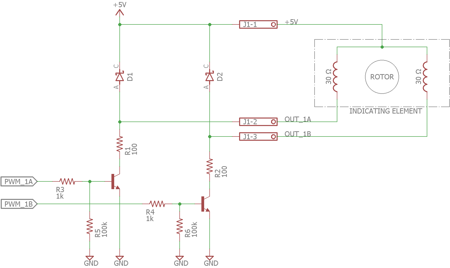
Example programmable current sink driver schematic.
The other option is to use programmable current sinks to control the currents through the dial’s coils. The schematic above shows two channels of programmable current sinks. I’ve used this design in the past to control IN-9 Nixie bargraph displays and some modern analog panel meters.
In 2018, Texas Instruments published a programmable low-side current sink circuit app note with all the details required to design and use this circuit. From the app note:
The programmable low-side current sink sets the current through a load based on the DAC output voltage. The current is sensed through RSET and the op amp biases a transistor to regulate the current through the load.
I selected the TI TLV5626 two-channel, voltage-output DAC to control the current sinks. The converter’s A channel controls the current through the dial’s left coil and the converter’s B channel controls the current through the dial’s right coil. R1 and R2 are the current sense resistors.
The design parameters for this use of the programmable current sink circuit are:
VCC = 5 V
IOUTMAX = 50 mA
RLOAD = 30 Ω
The DAC’s reference voltage can be selected from internal 1.024 V and 2.048 V sources. The maximum DAC output voltages for each of these two reference voltages according to the datasheet are:
For VREF = 1.024 V: VDACMAX = 2 × VREF × 0xFF0 ÷ 0x1000 = 2.040 V
For VREF = 2.048 V: VDACMAX = 2 × VREF × 0xFF0 ÷ 0x1000 = 4.080 V
According to the app note, we want to minimize the voltage across RSET so select
VREF = 1.024 V
VDACMAX = 2.040 V
With VCC, IOUTMAX, RLOAD, and VDACMAX defined, we can begin designing the circuit.
RSET = VDACMAX ÷ IOUTMAX = 2.040 V ÷ 0.050 A = 40.8 Ω
The closest 1% resistor value is 40.2 Ω. With the resistor selected, we need to calculate RLOADMAX to ensure we can reach IOUTMAX with the given VCC voltage:
RLOADMAX = (VCC – IOUTMAX × RSET) ÷ IOUTMAX = (5 – 0.05 × 40.2) ÷ .05 = 59.8 Ω
RLOAD is much less than RLOADMAX so the chosen values for VCC, IOUTMAX, and RSET work. Next compute the power dissipation through the transistor and RSET to compute the required power handling capability for these components:
PD(Q) = VCC × IOUTMAX – IOUTMAX2 × (RLOAD + RSET) = 0.073 W
PD(RSET) = IOUTMAX2 × RSET = 0.102 W
The transistor must be capable of handling at least 73 mW and the resistor capable of handling at least 102 mW. Let’s prototype the programmable current sink design.
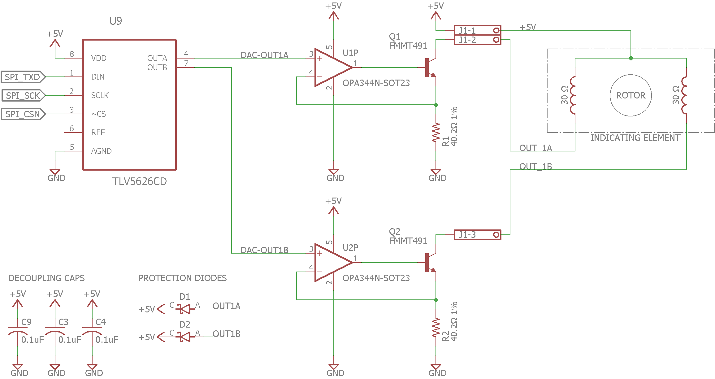
Programmable Current Sink Board
Instead of building the whole project at once, I started by prototyping just the current sink portion of the design. I learned a lot in the process of building the board, making measurements, and re-reading the TI DAC datasheet and TI app note while writing this blog post so there’s significant changes between the original schematic, what’s built, and what I’d do in the future.
Schematic
The primary design criteria for the original prototype of the programmable current sink board were:
- Run the DAC at VDD = 5 V with VREF = 2.048 V.
- Support a VIN range of 6.5 V to 24 V for the power to the indicators.
- Support controlling the DAC using both 3.3 V and 5 V microcontrollers.
- Support four channels of current sinks which is enough to drive two dials on the indicator at once.
- Fit in 4 square inches or less.
- Use parts I had on-hand or at least was familiar with.
- Once working, use two boards to drive all four dials.
The schematic below reflects these original design criteria:
schematic
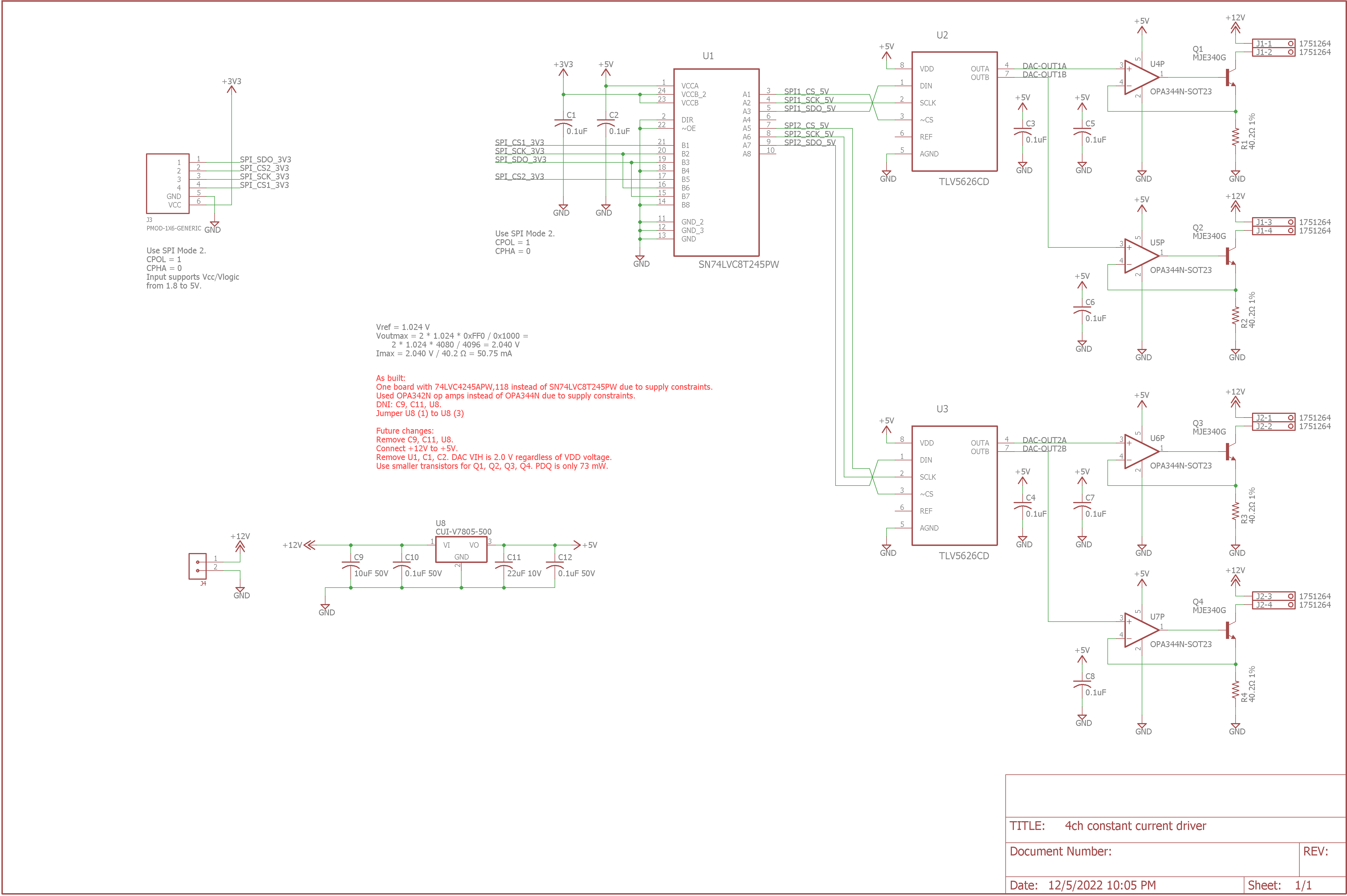
After building two of the boards to control all four dials and iterating through the design, I learned a few things:
- If I run the DAC with VREF = 1.024 V instead of 2.048 V, I only need a single 5 V power supply for everything and the current sense resistors drop from 82.0 Ω to 40.2 Ω.
- I only need about 250 mA current to control all four dials. At 5 V and 250 mA, the entire project can be a USB bus-powered design and the external power supply is not necessary.
- The TI TLV5626 DAC’s VIH is 2 V regardless of whether it is running from a 3.3 V or 5 V supply. This means that the level translation chips are not necessary.
- Some parts had to be substituted because they weren’t available due to the on-going component shortages.
With this new found knowledge, I reworked the boards to what’s shown in the “as-built” notes on the schematic:
- One board has an NXP 74LVC4245APW,118 instead of a TI SN74LVC8T245PW due to supply constraints. It’s easier to put the parts down even if they’re not needed than to jumper six wires on 12 pads on a TSSOP footprint on two boards.
- Both boards use OPA342N op amps instead of OPA344N op amps due to supply constraints.
- The voltage regulator (U8) and its large capacitors (C9 and C11) are not stuffed because they’re not necessary when running from a single 5 V supply.
- Jumper U8 (1) to U8 (3) to make VIN = VDD = 5 V.
And if I design new boards in the future, I came up with a list of changes for the next revision:
- Remove C9, C11, U8 because only a single 5 V supply is required.
- Connect +12V to +5V because VIN and VDD are both now 5 V.
- Remove U1, C1, C2 because the DAC’s VIH is 2.0 V regardless of the DAC’s VDD voltage.
- Use smaller transistors for Q1, Q2, Q3, Q4 because PDQ is only 73 mW.
- Add flyback protection diodes from VIN to each output.
- Build all 8 channels on a single board.
Layout
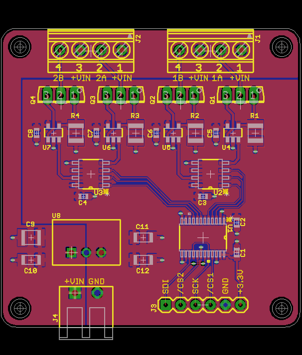
layout
The finished layout is shown in the image above.
Assembled Board

The assembled four channel programmable current sink board.
The photo above shows the board with all the modifications as described in the as-built section of schematic. Aside from a few parts not being stuffed and two pins on U8 being jumpered together, the board really doesn’t look too bodgy despite having some major changes from the original design.
Pico Control Board
After bringing up the programmable current sink boards successfully, it was time to make a board that directly interfaced a microcontroller to the current sink boards without a bunch of silly jumper wires. I used a Raspberry Pi Pico development board for initial bringup and decided to stick with that for the control board. I could have used a Microchip PIC16 or PIC18 or SiLabs EFM8 microcontroller just as easily.
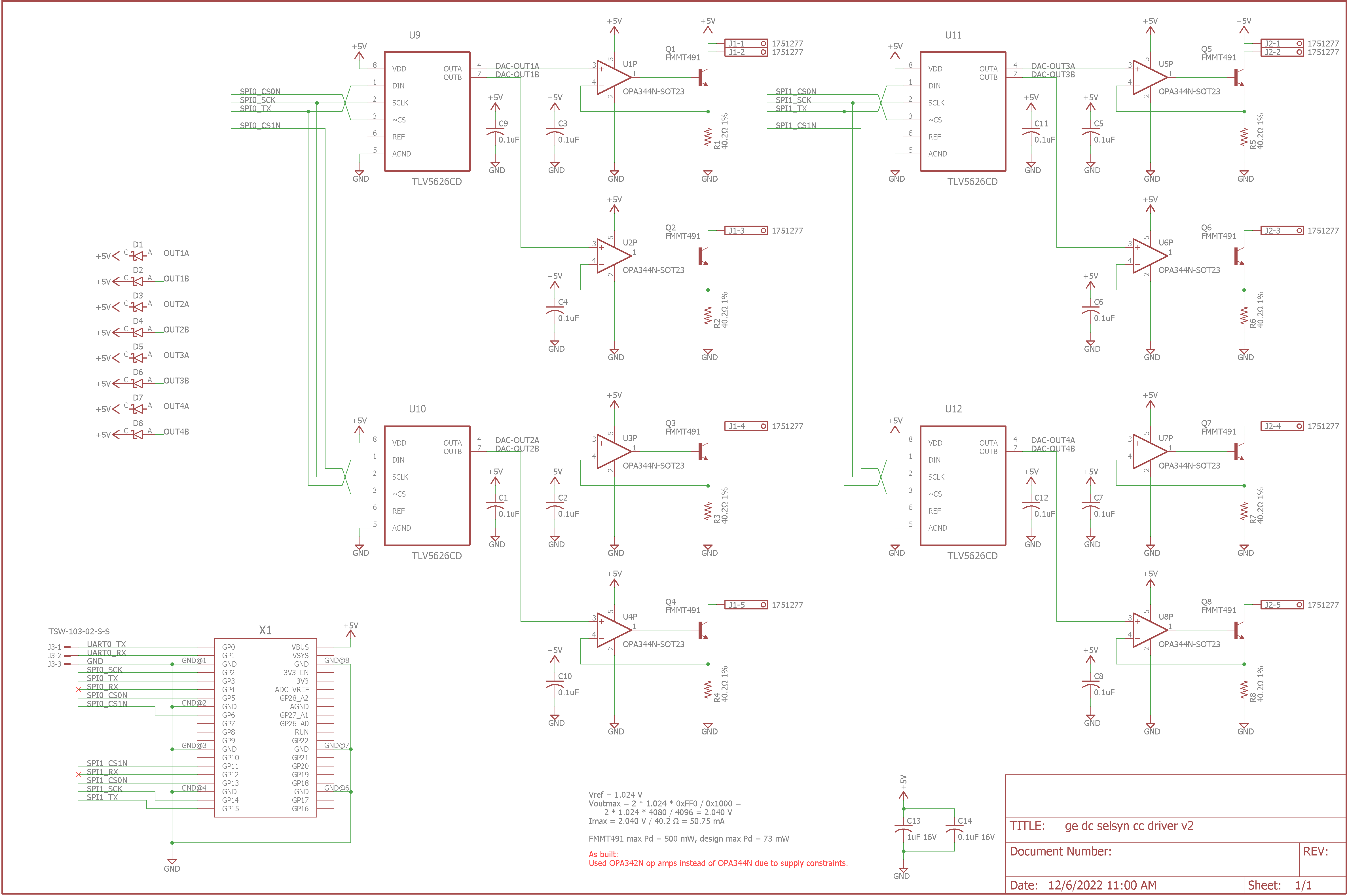
Schematic
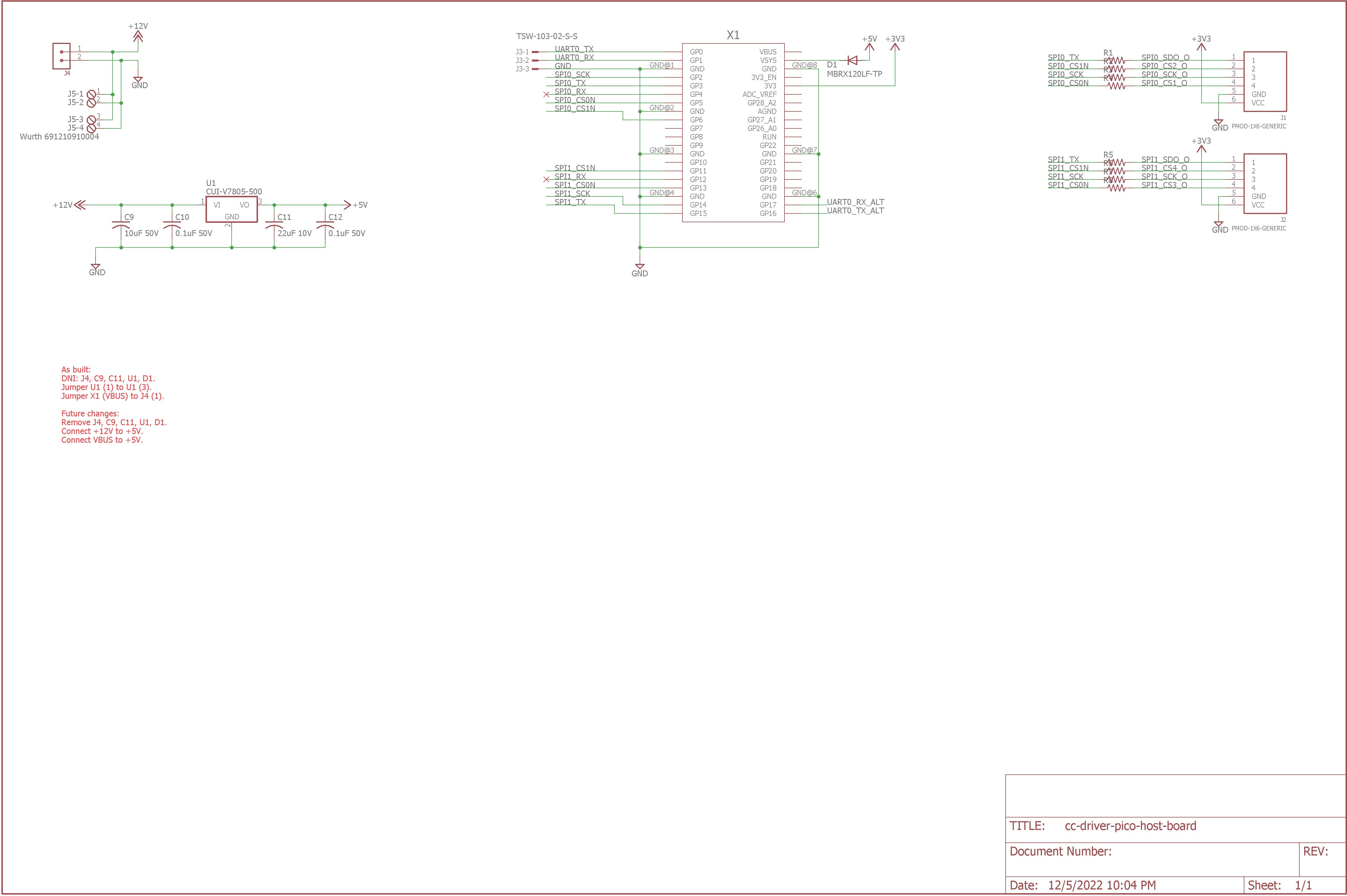
schematic
The schematic above reflects the original design before the decision to make the entire project powered by the USB bus instead of a separate external power supply. The as-built notes on the schematic describe the changes made to convert the board to a USB bus-powered design. The change made are:
- J4, C9, C11, U1, and D1 are not stuffed.
- U1 (1) is jumpered to U1 (3) using a short length of wire.
- X1 (VBUS) is jumpered to J4 (1) using a short length of wire.
On future revisions of this board, I’d:
- Remove J4, C9, C11, U1, and D1.
- Connect +12V to +5V because VIN and VDD are both now 5 V.
- Connect VBUS to +5V because the design is now USB bus-powered.
- Integrate the header sockets for the Pico development board on the same board as the programmable current sinks.
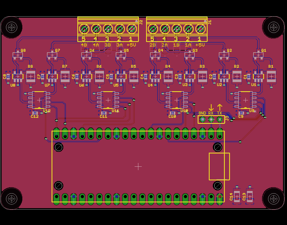
Layout
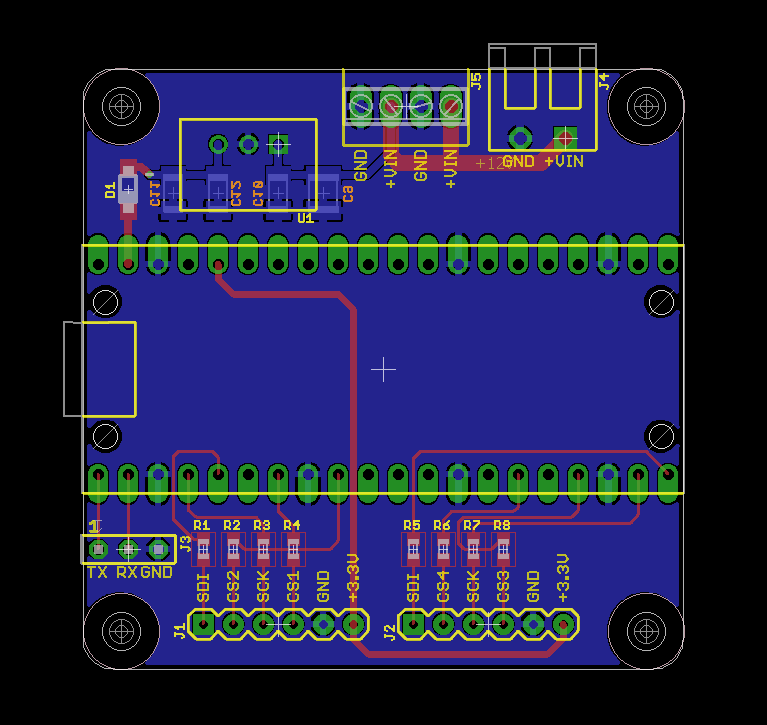
layout
The finished layout is shown in the image above. J5 is used to distribute power to the indicator and programmable current sink boards. J1 and J2 connect the SPI bus to each of the two programmable current sink boards. J3 is a console port for the Pico’s UART, printf debugging, and a very small command line interpreter I included in the C code.
Assembled Board
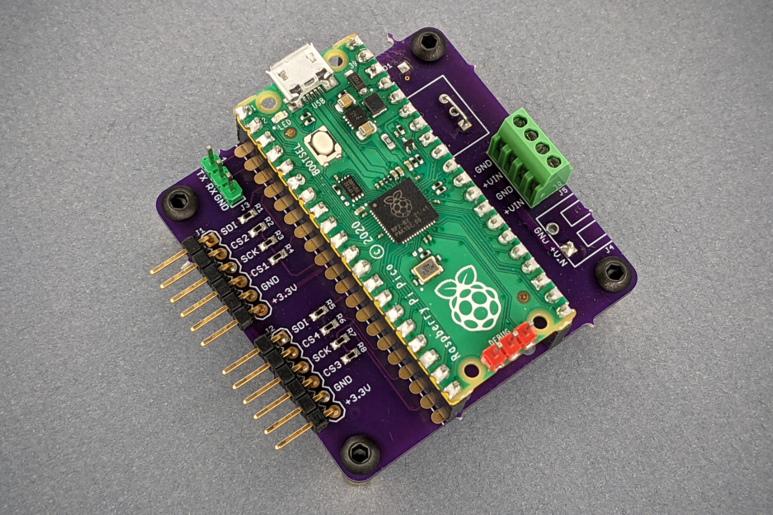
The assembled Raspberry Pi Pico-based control board.
The photo above shows the board with all the modifications as described in the as-built section of schematic. Aside from a few parts not being stuffed and two bodge wires, the board really doesn’t look too worse for wear despite multiple rounds of rework.
Raspberry Pi Pico Embedded Software
I used the RP2040 C SDK to develop the embedded software to control the indicator dials from a PC using USB.
TinyUSB and vendor-defined USB HID Devices
The RP2040 C SDK for the Pico development board includes the TinyUSB USB library. This library supports both USB host and USB device functionality and can be used to implement a variety of different USB device classes.
I modified the TinyUSB hid_generic_inout example included with the SDK to create my own vendor-defined USB HID device. Most of the modifications were in the usb_descriptors.c file but the tud_hid_set_report_cb callback in main.c had to be modified too.
VID / PID Changes
The first change in usb_descriptors. c was to give my project a unique USB vendor ID (VID) and product ID (PID). I picked something not quite random:
    .idVendor           = 0x4247, // vendor id - my poached vendor id
    .idProduct          = 0x0023, // product id - USB Gear and Flaps Indicators
USB Report Descriptor
The next modification was to create a USB report descriptor containing a single USB OUT report from the PC to the Pico to control the dials:
//--------------------------------------------------------------------+
// HID Report Descriptor
// a single OUT report with report ID of 1
// first byte is accept mask:
//   0x80 to accept dial 0 value
//   0x40 to accept dial 1 value
//   0x20 to accept dial 2 value
//   0x10 to accept dial 3 value
// bytes 2 to 5 are values for dials 0 to 3
//   0 turns indicator power off
//   valid range from 32 to 224
//   values below 32 are set 32
//   values above 224 are set to 224
//--------------------------------------------------------------------+

uint8_t const desc_hid_report[] =
{
    0x06, 0x00, 0xFF,  // Usage Page (Vendor Defined 0xFF00)
    0x09, 0x01,        // Usage (0x01)
    0xA1, 0x01,        // Collection (Application)

    0x85, 0x01,        //   Report ID (1)
    0x95, 0x05,        //   Report Count (5)
    0x75, 0x08,        //   Report Size (8)
    0x26, 0xFF, 0x00,  //   Logical Maximum (255)
    0x15, 0x00,        //   Logical Minimum (0)
    0x09, 0x01,        //   Usage (0x01)
    0x91, 0x02,        //   Output (Data,Var,Abs,No Wrap,Linear,Preferred State,No Null Position)

    0xC0              // End Collection
};
This USB report descriptor is a little different than the USB report descriptor in the engine cowl flaps indicator. This report descriptor consists of a single OUT report of five bytes. Byte 0 is a mask field. The upper four bits of this byte are accept bits. The lower four bits are not used. Bytes 1 to 4 are the dial position of the nose gear, right wing gear, flaps, and left wing gear respectively.
When an accept bit is 1, the corresponding dial will be updated with its corresponding dial value from bytes 1, 2, 3, or 4 of the OUT report. If the accept bit is 0, the corresponding dial will not be updated with the new dial value and will retain its existing value / position regardless of the value of its byte.
Serial Number Changes
The final change in usb_descriptors.c was to modify the routine that returns the USB descriptor strings when the request for the device’s serial number is queried:
uint16_t const* tud_descriptor_string_cb(uint8_t index, uint16_t langid)
{
    (void) langid;

    uint8_t chr_count;

    if (index == 0) {
        memcpy (&_desc_str[1], string_desc_arr[0], 2);
        chr_count = 1;
    } else {

        const char *str;
        char tmp[32];

        if (index == 3) {
            pico_get_unique_board_id_string (tmp, 32);
            str = tmp;
        } else {
            if (!(index < sizeof(string_desc_arr)/sizeof(string_desc_arr[0])) ) {
                return NULL;
            }
            str = string_desc_arr[index];
        }

        // Cap at max char
        chr_count = strlen (str);
        if (chr_count > 31) chr_count = 31;

        // Convert ASCII string into UTF-16
        for (uint8_t i = 0; i < chr_count; i++) {
            _desc_str[1+i] = str[i];
        }
    }

    // first byte is length (including header), second byte is string type
    _desc_str[0] =(TUSB_DESC_STRING << 8 ) | (2*chr_count + 2);

    return _desc_str;
}
Previously, the code always returned a fixed string for the serial number. This change uses the Pico SDK’s pico_get_unique_board_id_string function to return a hex string of the Pico board’s unique ID as the serial number. This didn’t strictly need to be done, but it’s kind of cool.
Set Report Callback Changes
The last big change was to the tud_hid_set_report_cb callback in main.cpp:
/---------------------------------------------------------------------------------------------
// TinyUSB HID Set Report callback
//

void tud_hid_set_report_cb(uint8_t itf, uint8_t report_id, hid_report_type_t report_type, uint8_t const* buffer, uint16_t bufsize)
{
    // this example doesn't use itf and report_type
    (void) itf;
    (void) report_type;

    for (int i = 0; i < bufsize; i++) {
        printf ("%02x ", buffer[i]);
    }
    printf ("\n");

    // check that we were called from hidd_xfer_cb in lib/tinyusb/src/class/hid/hid_device.c
    if (report_id == 0) {
        // check exactly six bytes in buffer
        if (bufsize == 6) {
            // check report id in first byte
            if (buffer[0] == 0x01) {
                if (buffer[1] & 0x80) {                // check mask
                    DacWriteLevels (0x01, buffer[2]);  // limit and send levels to dac a and B
                }
                if (buffer[1] & 0x40) {                // check mask
                    DacWriteLevels (0x02, buffer[3]);  // limit and send levels to dac a and B
                }
                if (buffer[1] & 0x20) {                // check mask
                    DacWriteLevels (0x04, buffer[4]);  // limit and send levels to dac a and B
                }
                if (buffer[1] & 0x10) {                // check mask
                    DacWriteLevels (0x08, buffer[5]);  // limit and send levels to dac a and B
                }
            }
        }
    }
}
This code checks the report ID and the buffer size then implements the USB OUT report described in the USB report descriptor.
Controlling the DACs
The DACs are controlled using the Pico’s two SPI peripherals and four active-low chip select lines.
DacWriteLevels
The DacWriteLevels function takes a mask of which DACs to write and a dial value. It sets the corresponding DAC’s A channel to the dial value. It sets the corresponding DAC’s B channel to 256 minus the dial value. This way when the dial’s left coil current ramps up, its right coil current ramps down and vice versa. If the channel value is 0, it sets both DAC channels to 0 effectively shutting down the dial and causing the dial to spring to its OFF position.
//---------------------------------------------------------------------------------------------
// DacWriteLevels
//
// write levels to the selected DAC(s)
//

void DacWriteLevels (uint8_t select_mask, uint8_t level)
{
    uint8_t dacA, dacB;

    // convert a dial value to DAC levels
    dacA = level;
    dacB = 256 - dacA;

    // write dacA and dacB
    dacWrite2 (select_mask, 0x00 | ((dacB >> 4) & 0x0f),   // write buff and dac B
                            0x00 | ((dacB << 4) & 0xf0));
    dacWrite2 (select_mask, 0x80 | ((dacA >> 4) & 0x0f),   // write A, mv buf to B
                            0x00 | ((dacA << 4) & 0xf0));
}
dacWrite2
The dacWrite2 function does the dirty work of figuring out the active chip selects, figuring out the active SPI peripherals, then writing two bytes of data to the selected DAC(s):
//---------------------------------------------------------------------------------------------
// dacWrite2
//
// write two bytes to up to four DACs at a time
//

void dacWrite2 (uint8_t select, uint8_t a, uint8_t b)
{
    // printf ("%02x %02x\n", a, b);

    // CS low
    asm volatile ("nop \n nop \n nop");
    if (select & 1) {
        gpio_put (SPI0_CS0n_PIN, 0);
    }
    if (select & 2) {
        gpio_put (SPI0_CS1n_PIN, 0);
    }
    if (select & 4) {
        gpio_put (SPI1_CS0n_PIN, 0);
    }
    if (select & 8) {
        gpio_put (SPI1_CS1n_PIN, 0);
    }
    asm volatile ("nop \n nop \n nop");

    // transfer data
    if (select & 3) {
        spi_write_blocking (spi0, &a, 1);
        spi_write_blocking (spi0, &b, 1);
    }
    if (select & 12) {
        spi_write_blocking (spi1, &a, 1);
        spi_write_blocking (spi1, &b, 1);
    }

    // CS high
    asm volatile ("nop \n nop \n nop");
    gpio_put (SPI0_CS0n_PIN, 1);
    gpio_put (SPI0_CS1n_PIN, 1);
    gpio_put (SPI1_CS0n_PIN, 1);
    gpio_put (SPI1_CS1n_PIN, 1);
    asm volatile ("nop \n nop \n nop");

    // enforce a small delay between writes
    asm volatile ("nop \n nop \n nop");
    asm volatile ("nop \n nop \n nop");
    asm volatile ("nop \n nop \n nop");
    asm volatile ("nop \n nop \n nop");
    asm volatile ("nop \n nop \n nop");
}
C# .NET Windows Forms App
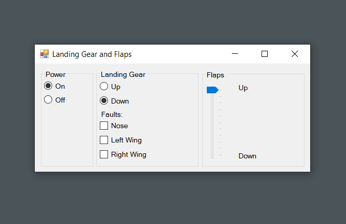
The Visual Studio 2019 C# .NET Windows Forms app for controlling the indicators.
The screen capture above shows the C# .NET Windows Forms app used to control the flaps and landing gear indicator. It’s divided into three main sections: Power, Landing Gear, and Flaps.
Power
The leftmost pane controls power to the meter. When the power is off, the current sinks are set to 0 mA and the dials spring to their off position. When the power is on, the current sinks are enabled and the dials are set to the landing gear and flaps positions controlled by the next two panes in the dialog box.
Landing Gear
Changing the landing gear position in the middle pane causes the all the landing gear to move slowly from their current position to either the up and locked or down and locked position as selected. Selecting one of the fault boxes under the up / down control will cause the correspond landing gear to stop moving and get stuck wherever it is. Deselecting the fault box will enable the gear to move toward its target position again.
Flaps
The rightmost pane controls the flaps dial. Sliding the track bar up and down will raise and lower the flaps accordingly. The track bar can be set at any position between up and down to extend the flaps by only that amount.
Putting it All Together
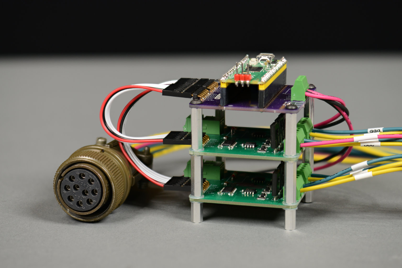
Boards wired and ready to go!
The photo above shows all the boards stacked together and connected. The red/black/white wires are the SPI buses from the Pico to the two programmable current sink boards. The red/yellow/blue wires are the supply voltage and current sink outputs to the Bendix connector to the meter. The red/black wires at the top of the board are the USB VBUS supply voltage to the two programmable current sink boards.
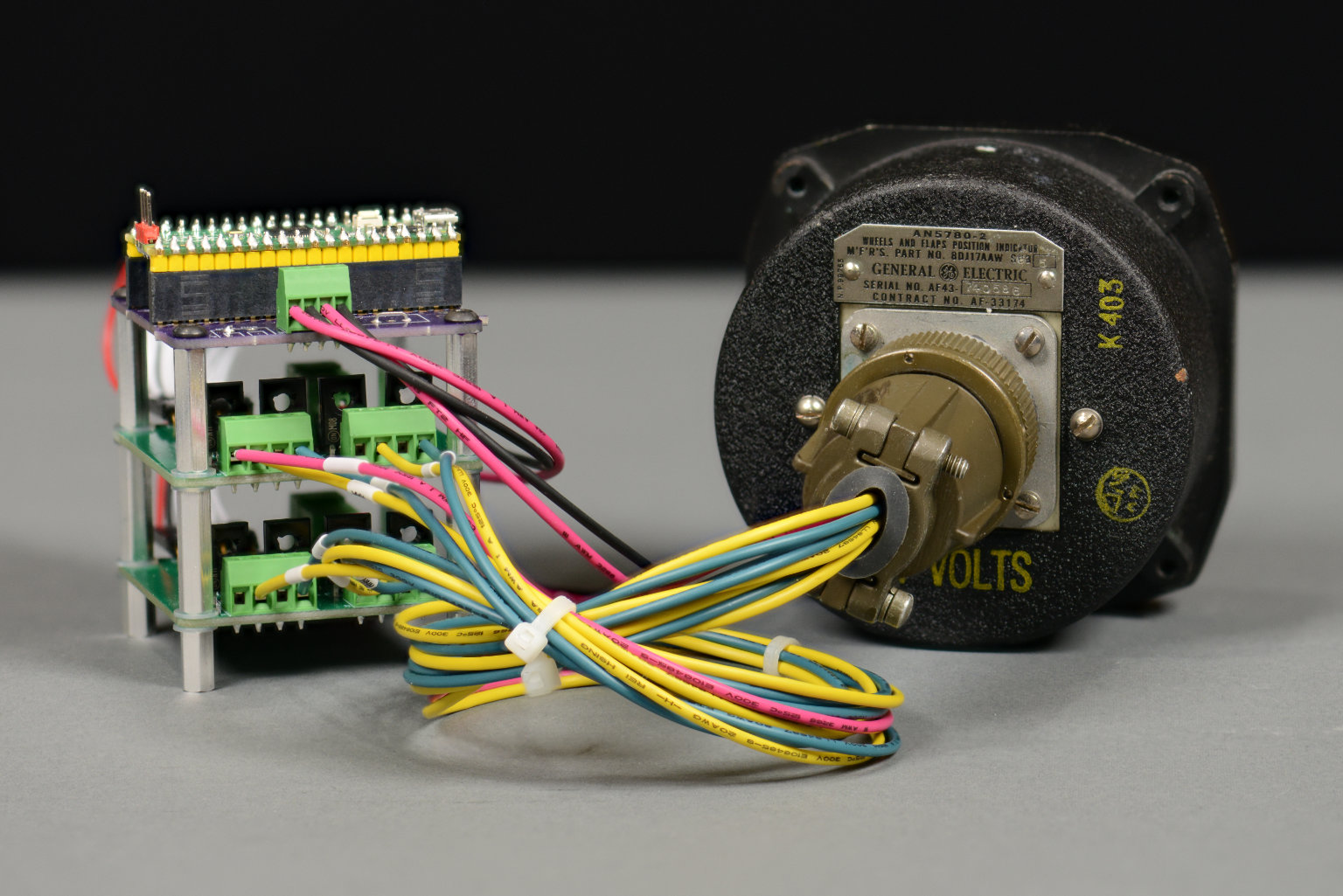
The board stack connected to the back of the indicator.
The photo above is another view of the board stack. This time with the connector connected to the back of the meter.
And finally, a quick video demonstrating the entire project including the C# GUI!
Updated Board Design
Based on what I learned while building this project, I created a new board design. The schematic and layout of these boards follow. These designs have not been tested and I’m highly unlikely to build a board, buy parts, and assemble them myself.
Schematic
Updated schematic incorporating all I learned on this project.
The schematic of the updated but untested board design is shown above.
Layout
Updated board layout incorporating all I learned on this project.
The layout of the updated but untested board design is shown above.
Design Files
The board design, Pico source code, and C# source code for this project are available on Github in my usb-ww2-gear-and-flaps repository.