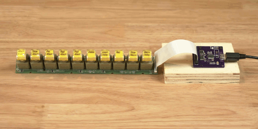
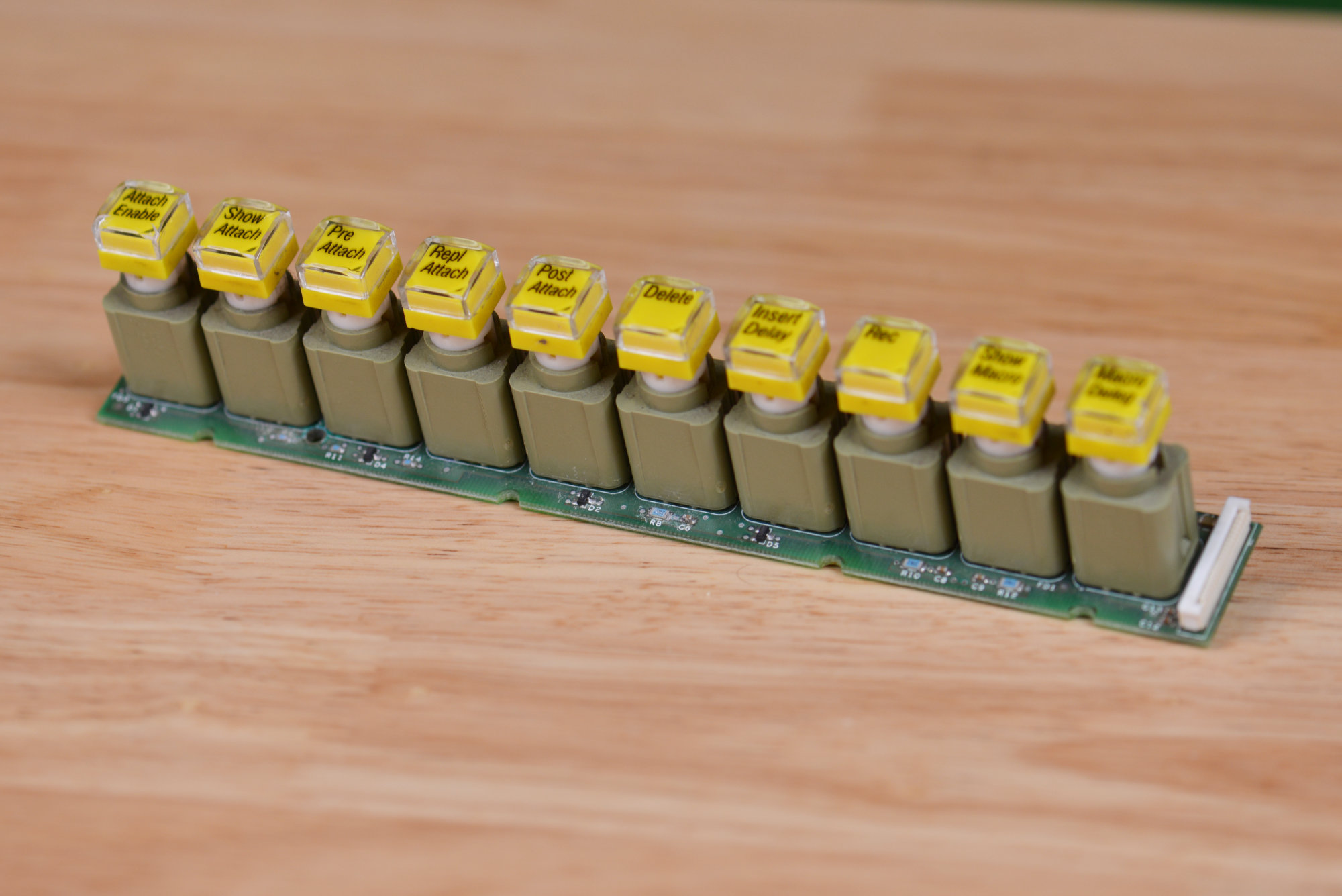
The resurrected Grass Valley user definable switch panel.
In this project, I convert a set of illuminated push buttons from a vintage Grass Valley video mixer into a custom vendor-defined USB HID peripheral. Like the USB analog panel meters project, this project uses a Silicon Labs EFM8UB1 microcontroller for USB connectivity. Unlike the panel meters project which only received data from the USB host, this project needs to send data back to the USB host too.
In this write up, we’ll reverse engineer the button panel, decide on a strategy for reading the keys and controlling the LEDs, build a board, then write both embedded and Linux software to interface with the button panel. If you want to build your own device like this but don’t have this specific switch panel, don’t worry–the ideas presented here are applicable to any generic 3×4/4×3/4×4 matrix keypad with or without LEDs.
The Button Panel’s Lineage
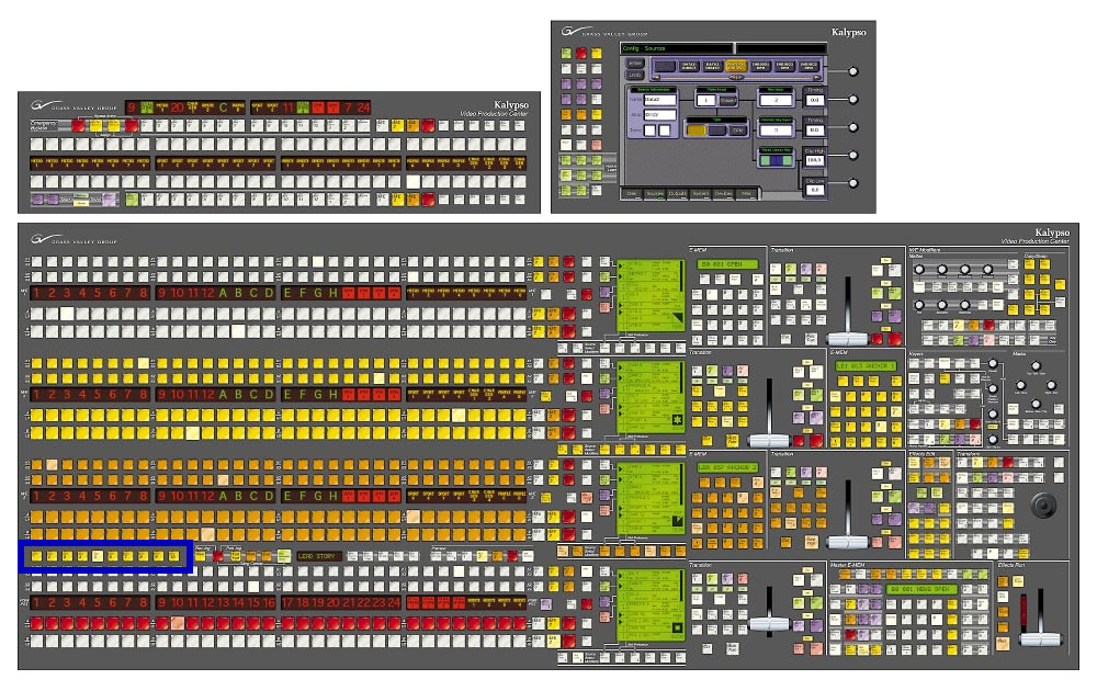
The location of the user definable switches panel on a Grass Valley Kalypso 4-M/E control surface. Image from manufacturer’s preliminary data sheet circa 2000.
The button panel I used in my project is the user definable switches panel from a Grass Valley Kalypso 4-M/E video mixer control surface. I highlighted the location of the user definable switches on the 4-M/E control surface in blue on the above image from the panel’s preliminary data sheet.
The 4-M/E control surface is a giant remote control for the video switcher frame. The technical director uses the control surface in the production studio’s control room to instruct the video switcher frame as to how to mix the available video sources from the studio together. The frame does the actual video mixing and is located in a machine room away from the production studio.
The control surface has hundreds of buttons, hundreds of LEDs, and dozens of displays. All these inputs and outputs need to make their way back and forth between the control surface and the video switcher frame. In a future post, we’ll look at how all these inputs and outputs get into the single board computer inside the control surface and to the frame, but for now, we’re going to focus on the inputs, outputs, and construction of the small 10-key user definable switches panel.
Up Close with the Button Panel
Close up of the button panel. Just some buttons, resistors, capacitors, and SOT-23 mystery packs.
When I acquired the user definable switches panel, I did not know exactly how it worked or if it would even be useful as is. I figured worst case I could remove the buttons and use them on my own board. To find out if it could be useful as is, it was time to learn as much as possible about the button panel. This started with a detailed examination of the board and the parts on the panel then mapping how the parts were connected to each other.
The Buttons!
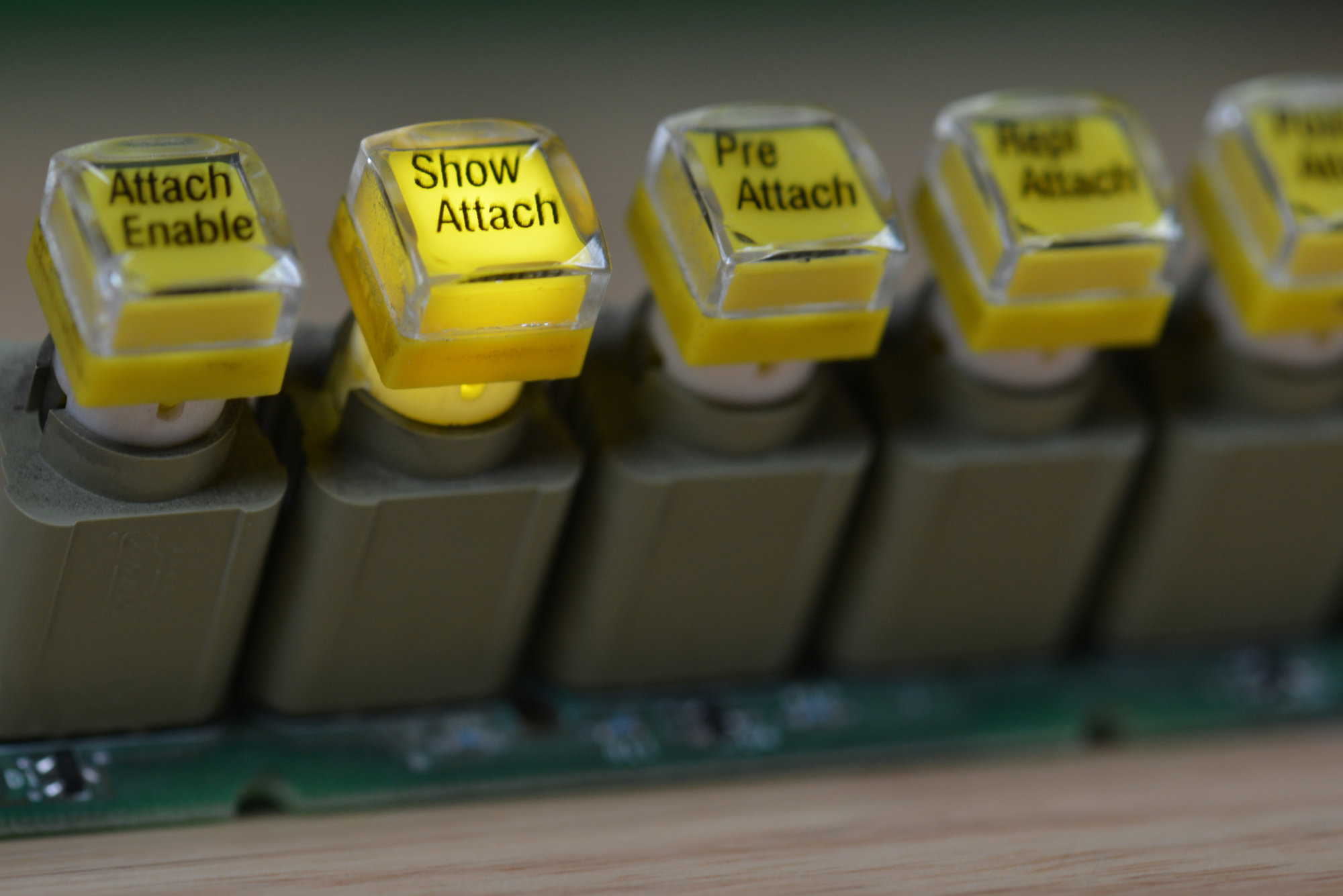
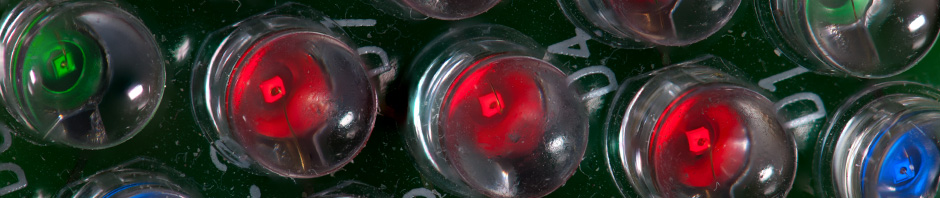
These buttons still look and work great after 15 years!
Let’s be honest, the reason I acquired the panel was for the buttons. These things are incredible. They’re a bit firmer than a mechanical keyboard button but still have 4 or 5 mm of travel and are quite springy when released. Each button has an internal LED for illumination. The key caps are removable from the switch and the clear lid is removable from the key cap. These lids have their labels printed on the inside of them but with a set of blank key caps, you could laser print your own labels on transparency film.
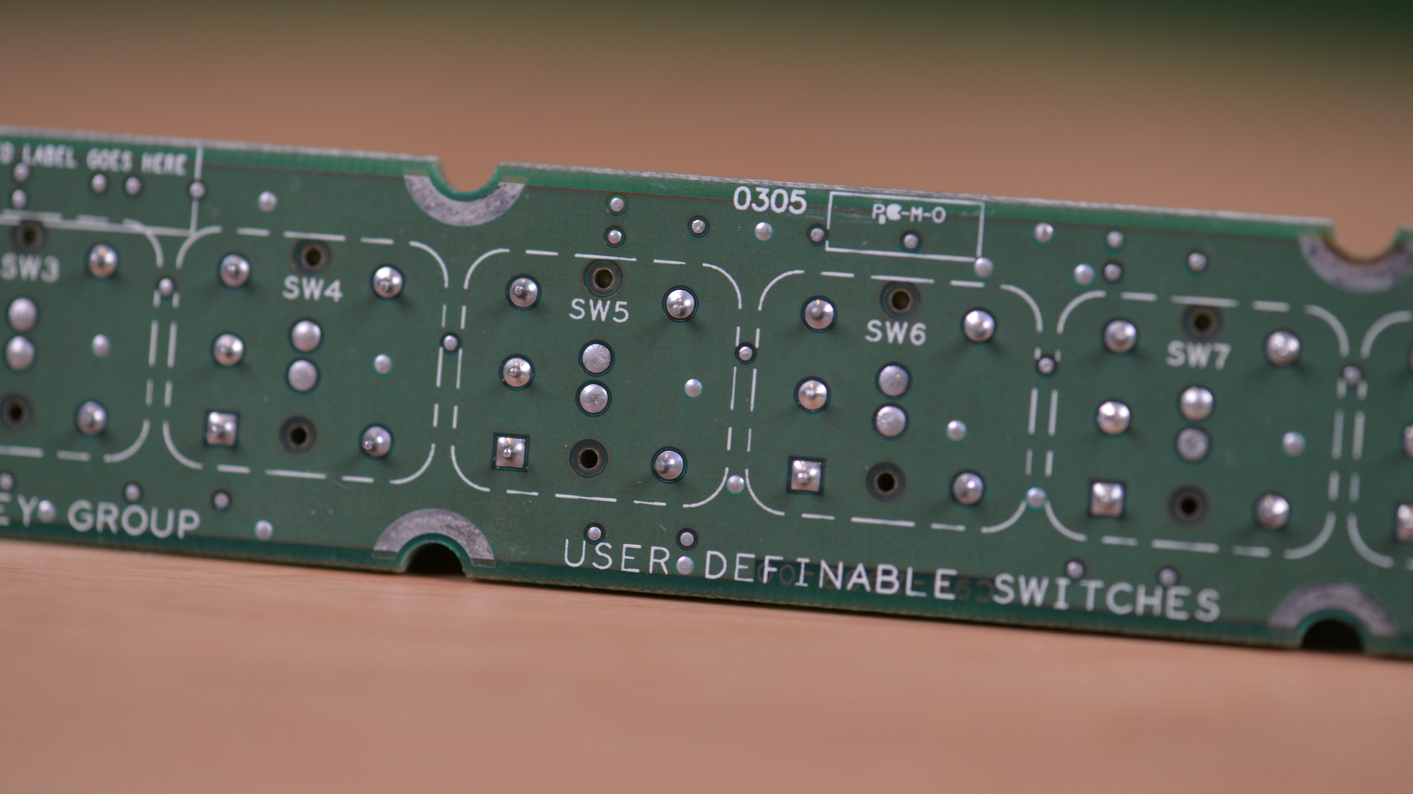
Rear view of the switch panel.
Each switch has a ton of pins. As best I can tell, only four are connected. The rest are for mechanical stability. The square pad in the bottom left is attached to the switch’s column in the switch matrix. The round one just above it is connected to the switch’s row through a diode in the switch matrix. The two in the middle are the LED. The bottom is the LED anode and the top is the LED cathode. The top left, top right, and bottom right pins do not appear to be connected or are redundant connections to the LED.
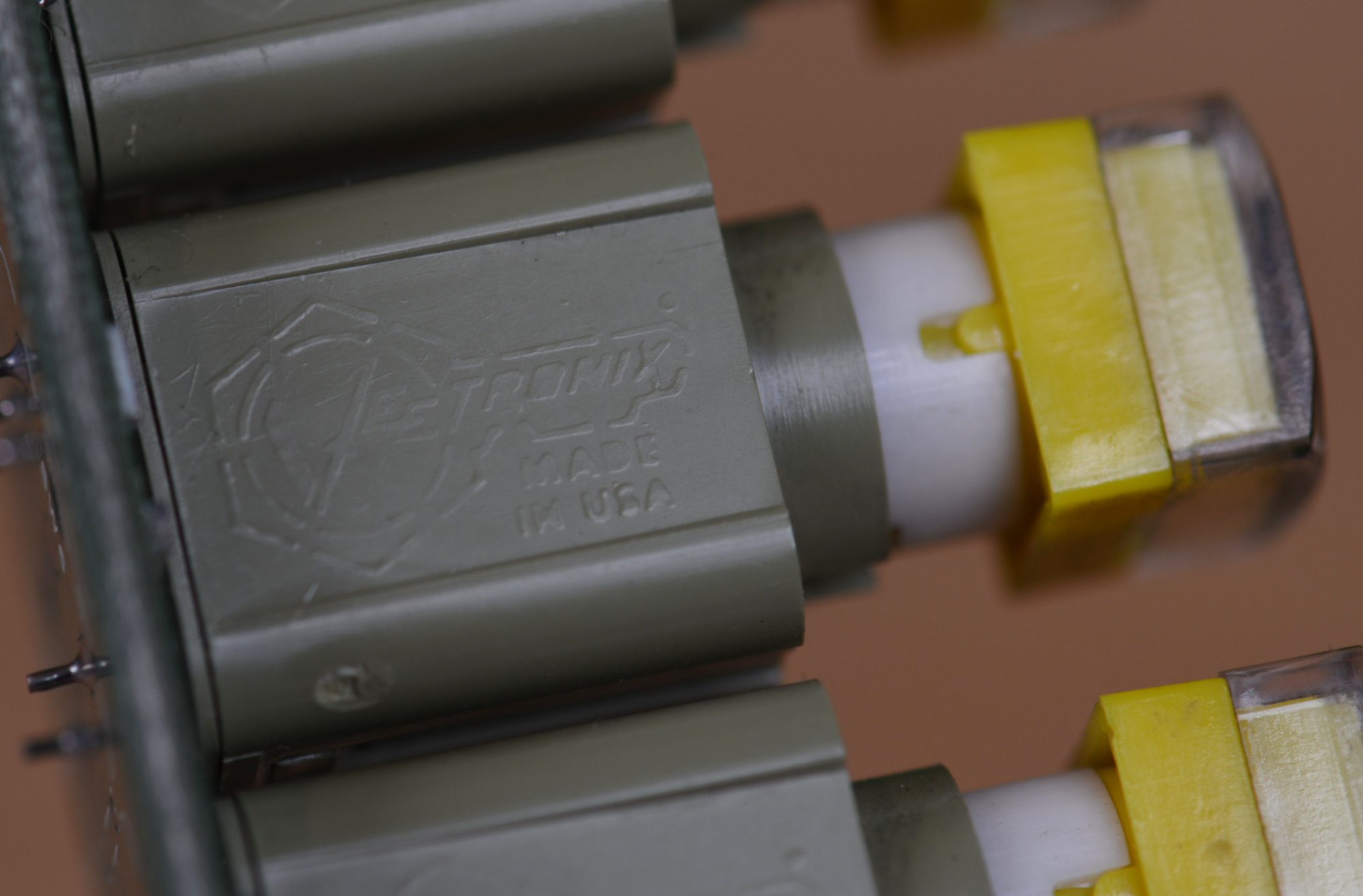
At last! The name of the manufacturer!
One of the big mysteries was who made these switches. Googling the part numbers printed on the side of the switches turned up no results. On older equipment from the 70s and 80s, Grass Valley used switches from Electro-Mech Components. Electro-Mech did not have anything like these switches on their website.
One day I noticed a faint pattern on the side of the switches. If the side of the switch caught the light just right, you could see a faint “VEETRONIX” logo along with the text “MADE IN USA.” A quick Google search, and I had my answer: they’re made by a company called Veetronix in Lexington, Nebraska. Taking a look at their website confirmed that these are indeed their switches.
I pulled up a datasheet for the current model of switch that looked the closest to these switches. There was an ominous sounding warning in the datasheet:

An ominous sounding warning in the datasheet.
With a bit more research, I learned that these switches use magnetic reed switches instead of traditional electrical contacts to make and break the circuit when the switch is pushed and released. If the switches are located next to strong magnetic fields, they’d get stuck in the on position and would not function as switches.
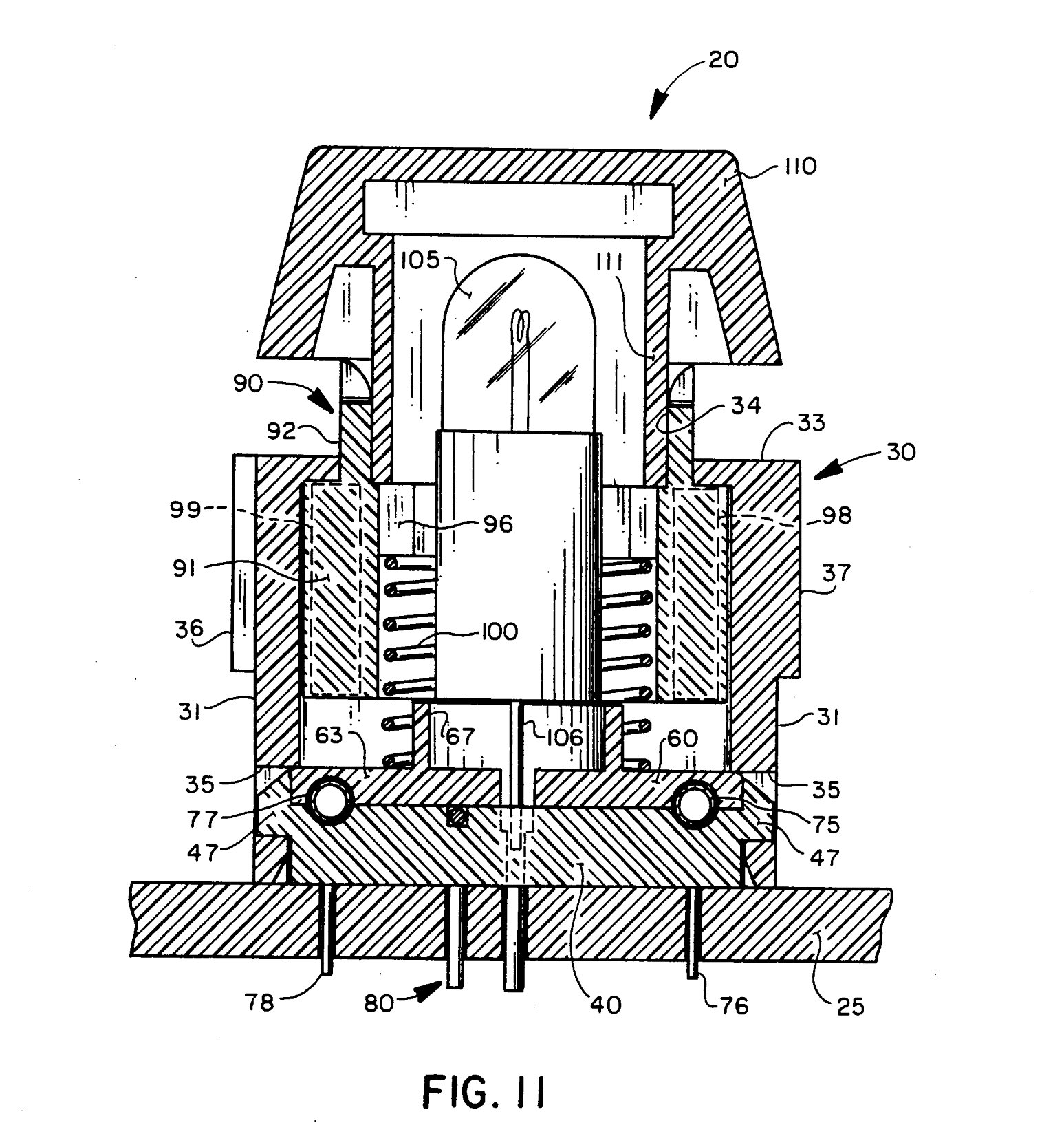
Figure 11 from US patent 5,057,807. The important parts are magnets 98 and 99 and reed switches 75 and 77.
With a bit more digging, I found US patent 5,057,807 issued to Veetronix in Lexington, Nebraska, on October 15, 1991. The patent cites an earlier patent for a push button switch with magnetic reed contacts going all the way back to 1973. The patent has a ton of text, figures, and claims, but figure 11, reproduced above, is the most interesting part of the patent.
In figure 11, the reed switches, 75 and 77, lie horizontal in the switch base while the magnets, 98 and 99, fit into vertical cavities in the switch plunger. When the switch is depressed, the magnets move toward the reed switches causing them to close. When the switch is released, the plunger and magnets are returned to their rest position by a spring, 100, thus opening the switch. In the middle of the switch is a cavity for an incandescent bulb or LED.
The Connector
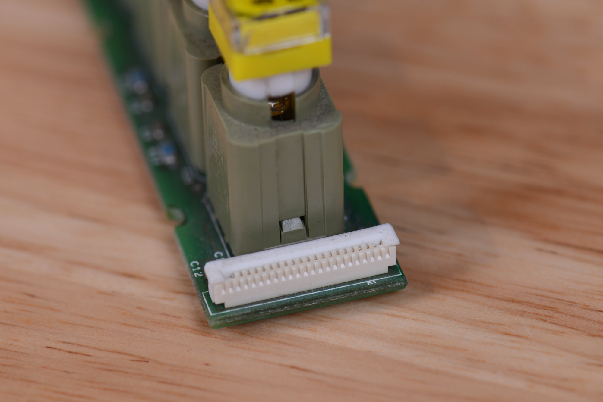
20-pin, 1mm pitch flex cable connector.
While nowhere near as exciting as the buttons, this board has a connector on its right hand side that connected to the rest of the electronics in the control surface. Ideally, I could connect my electronics to that connector and use the board as-is without any modifications. I measured the pitch as 1mm and found a similar connector on Digi-Key, Amphenol part number SLW20S-1C7LF. I ordered a few and confirmed that they fit the short flex cable that came with the buttons.
Other Parts

More dirt than parts along with a few SOT-23 mystery packs.
The board has a few other parts. There’s four 5k resistors, ten 39 ohm resistors, a bunch of small capacitors, and five SOT-23 mystery packs with the text “A4″ stamped on top of them.
Piecing Together the Schematic
Mapping Connectivity
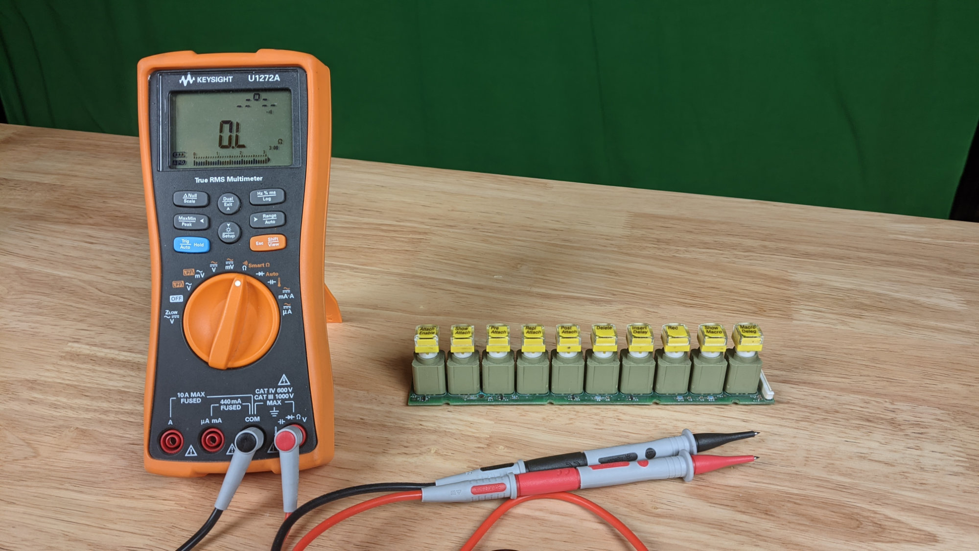
Yep, really no other way to do it. Grab a DMM and set it for continuity test. Diode test can be useful too.
The next step is always time consuming. I used a Keysight U1272A DMM with continuity and diode test functions to map out the connections on the circuit board. The diode test is useful for figuring out the polarity of diodes and LEDs. The focus was to figure out how the keys and LEDs are connected to the 20-pin connector on the right-hand side of the board.
The key is to take good notes then immediately document your findings in a final, readable format. Otherwise, you end up repeatedly tracing the same circuits over and over again. While not too bad for a board this size, repeating your measurements can be quite a waste of time on larger, more complicated boards. I eventually turned my notes into an almost complete schematic of the button panel.
The Mostly Complete Button Panel Schematic
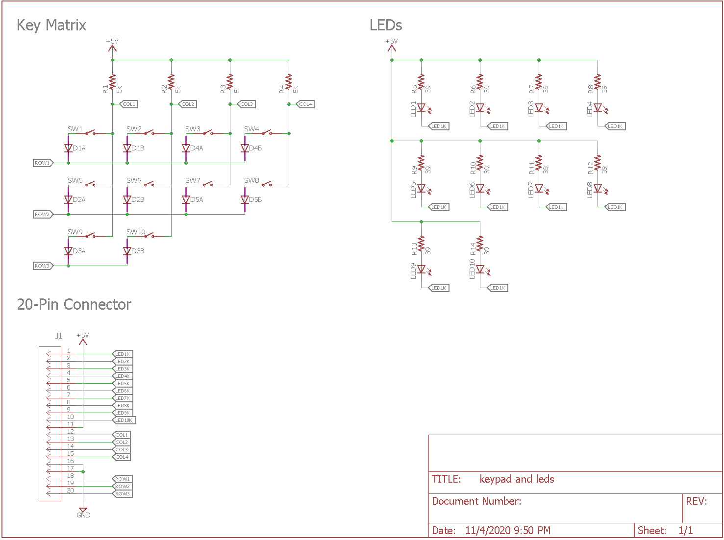
Schematic of the button panel. The buttons and LEDs are integrated units but the LEDs are shown here separately for clarity.
After a few hours of work, I managed to piece together a mostly complete schematic. The buttons are arranged in a matrix with four columns and three rows. The columns and rows are connected to the 20-pin connector. Each column has a 5k pullup resistor to +5V. Each switch is connected to a column and then to a row through a diode.
The SOT-23 mystery packs ended up being BAV70LT1G dual switching diodes. Each package has two diodes with a common cathode. One key connects to the first diode’s anode, the key next to it connects to the second diode’s anode, and then the common cathode connects to the row line.
The LEDs are arranged in a common-anode configuration. Each LED’s anode is connected to a common +5V power rail through a 39 ohm series resistor. Each LED’s cathode is connected to a pin on the 20 pin connector. The capacitors on the board just connect between the 5 volt power rail and ground and are not shown on the schematic.
Making Some Design Decisions
For this project, the major design decisions included how to scan the key matrix, how to control the LEDs, and what USB microcontroller to use. This project predates my analog panel meters project so I was still using micro USB connectors rather than USB Type C connectors at the time.
Scanning The Buttons
Looking at the schematic for the button panel in the section above, scanning the key matrix to read which keys are pressed requires seven digital GPIO pins and a +5V power supply for the column pullup resistors. The GPIO pins are split into a group of four column pins and a group of three row pins.
To scan the key matrix and determine which keys are pressed, the column pins are set to inputs and the the row pins are brought low one pin at a time. The state of the column pins is then read. If a key in the active row is pressed, the column pin connected to the pressed switch will read low. If a key is not pressed, the column pin will read high. This procedure is then repeated until all three rows have been scanned. Once all the rows are scanned, you know the state of every key in the matrix. For a more detailed explanation of scanning a matrix keypad, I recommend this tutorial.
Our microcontroller will need four input pins to connect to the column signals and three open-drain output pins to connect to the row signals. On a keypad without diodes between the keys, using open-drain outputs prevents shorts between ground and the power rail if two keys are pressed simultaneously. In addition, the column signals are hardwired to +5V through 5k resistors so the row and column lines on the microcontroller need to be 5V tolerant.
Controlling The LEDs
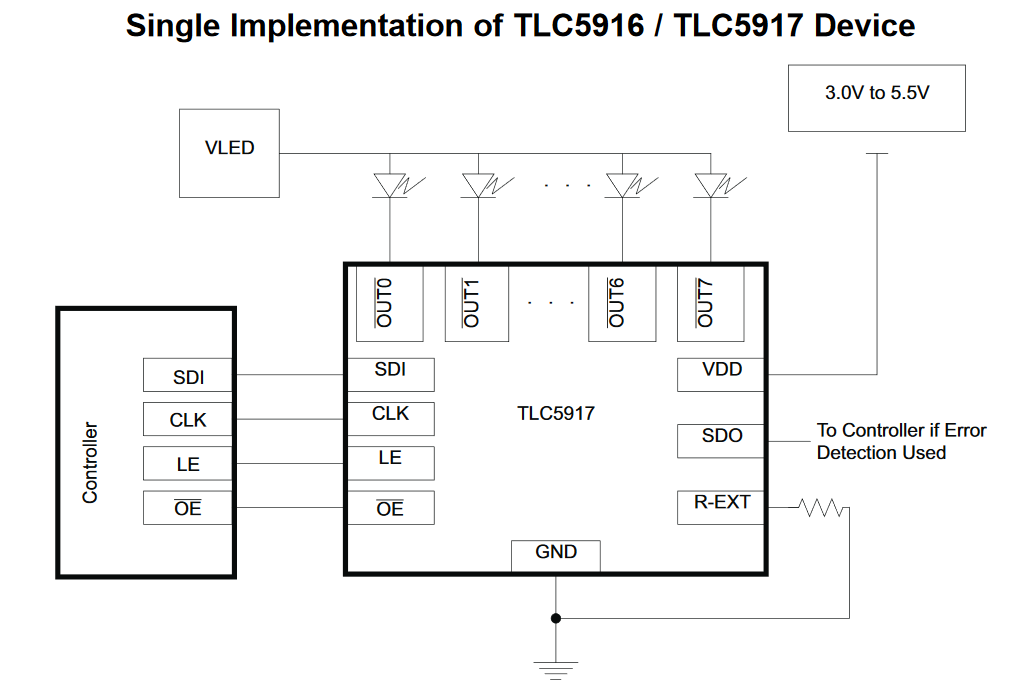
Block diagram of the TLC5916 eight-channel, constant-current LED driver IC from the datasheet.
To control the LEDs, I’m going to use one of my favorite LED driver chips, the Texas Instruments TLC5916. The TLC5916 is an eight-channel, constant-current LED sink driver. This chip allows a microcontroller to control up to eight LEDs using only three or four pins and allows the the forward current for all the attached LEDs to be set using a single resistor. Multiple chips can be cascaded together to control even more LEDs without using any more microcontroller pins. Since we have 10 LEDs to control, we’ll need two of these chips.
If you refer back to the schematic for the button panel, you’ll notice 39 ohm resistors in series with each LED. The resistors limit the current to each LED, but they don’t limit the current enough. If we assume a 5 volt power supply and a forward voltage of 3.5 volts for a typical white LED, the 39 ohm resistors only limit the current to (5 – 3.5) / 39 = 38 mA. This is enough current to destroy the LED. Using a current setting resistor of 1.2k with the TLC5916 will bring the LED operating current down to a more reasonable 16 mA.
The Silicon Labs EFM8UB1

EFM8UB1 functional block diagram from the data sheet.
For this project, I’m going to use the Silicon Labs EFM8UB1 USB microcontroller. The EFM8UB1 is an 8-bit 8051-based microcontroller featuring the usual assortment of microcontroller peripherals such as SPI and I2C as well as USB device capabilities. It runs from 3.3 volts, includes a built-in 3.3 volt voltage regulator, and has five-volt tolerant I/O. It includes two built-in oscillators and the 48 MHz oscillator features USB clock recovery. A complete full-speed, 12 Mbps, USB device can be built using just this microcontroller and four decoupling capacitors.
The EFM8UB1 has 16 kB of FLASH and 2,304 bytes of RAM. It’s available in QFN-20, QFN-28, and QSOP-24 packages. I’m going to use the QSOP-24 because it’s easier for me to hand solder leaded packages than leadless packages. If your application outgrows the EFM8UB1, Silicon Labs has a migration path to the EFM8UB2 for applications needing more pins and memory or the EFM8UB3 for space-constrained applications that just need more memory.
For software development, the EFM8UB1 uses the Eclipse IDE and the Keil 8051 compiler in a software package called Simplicity Studio. Silicon Labs has negotiated a free license for the full version of the Keil 8051 compiler for use with their devices. The free, fully-optimizing compiler license gives the Silicon Labs EFM8 parts a significant advantage over devices from other manufacturers that require a monthly subscription to access the full versions of their compilers.
Designing the USB Controller
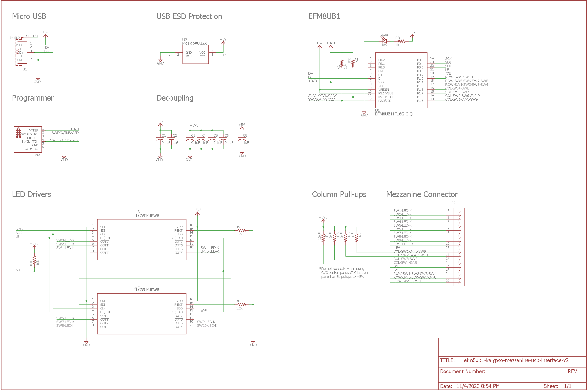
USB interface board for the user definable switches panel.
The top half of this schematic is common to most EFM8UB1 USB designs. There’s a USB connector, ESD protection for the USB signals, a programmer/debugger connection, decoupling capacitors, and the EFM8UB1 microcontroller itself. The bottom half of the schematic contains the circuitry unique to this project. There are two TLC5916 LED drivers to drive the 10 LEDs on the button panel and there’s a 20-pin connector to connect to the flex cable that connects to the button panel.
I used the Silicon Labs’ Simplicity Studio IDE to determine the crossbar settings to move the SPI interface to the right hand side of the chip. This side of the chip is easier to route PCB traces out of because it is away from the USB interface and voltage regulator pins and their decoupling capacitors. For more information on the EFM8UB1 crossbar switch, see the “Fixing the Pin Out” section of my USB analog panel meters post.
The SCK clock output on the EFM8UB1 micrcontroller is connected to the SCK clock inputs on both TLC5916 drivers. The EFM8UB1 SDO pin connects to the SDI pin on the first TLC5916. The SDO pin on the first TLC5916 then connects to the SDI pin on the second TLC5916. The SDI pin on the EFM8UB1 is not connected.
The next two pins on the right-hand side of the EFM8UB1 are set up as push-pull outputs. One connects to both TLC5916’s latch enable inputs and the other connects to both TLC5916’s active-low output enable pins. The output enable signal has a pullup to +3.3V to keep the LEDs off until the microcontroller has initialized the TLC5916’s and pulled the output enable signal low.
Below the connections to the TLC5916 drivers on the EFM8UB1 are the connections to the key matrix. Port one pins P1.0 , P1.1, and P1.2 are set as open-drain outputs and connected to the row pins. P1.3 to P1.6 are set as inputs and connected to the column pins. The column pins already have 5k pullup resistors to +5V on the button panel so the 3.3V 10k pullup resistors on our board should not be populated. Since the EFM8UB1 has five-volt tolerant I/O, the button panel’s pullups to +5 volts will not cause damage to the EFM8UB1.
Designing the Board
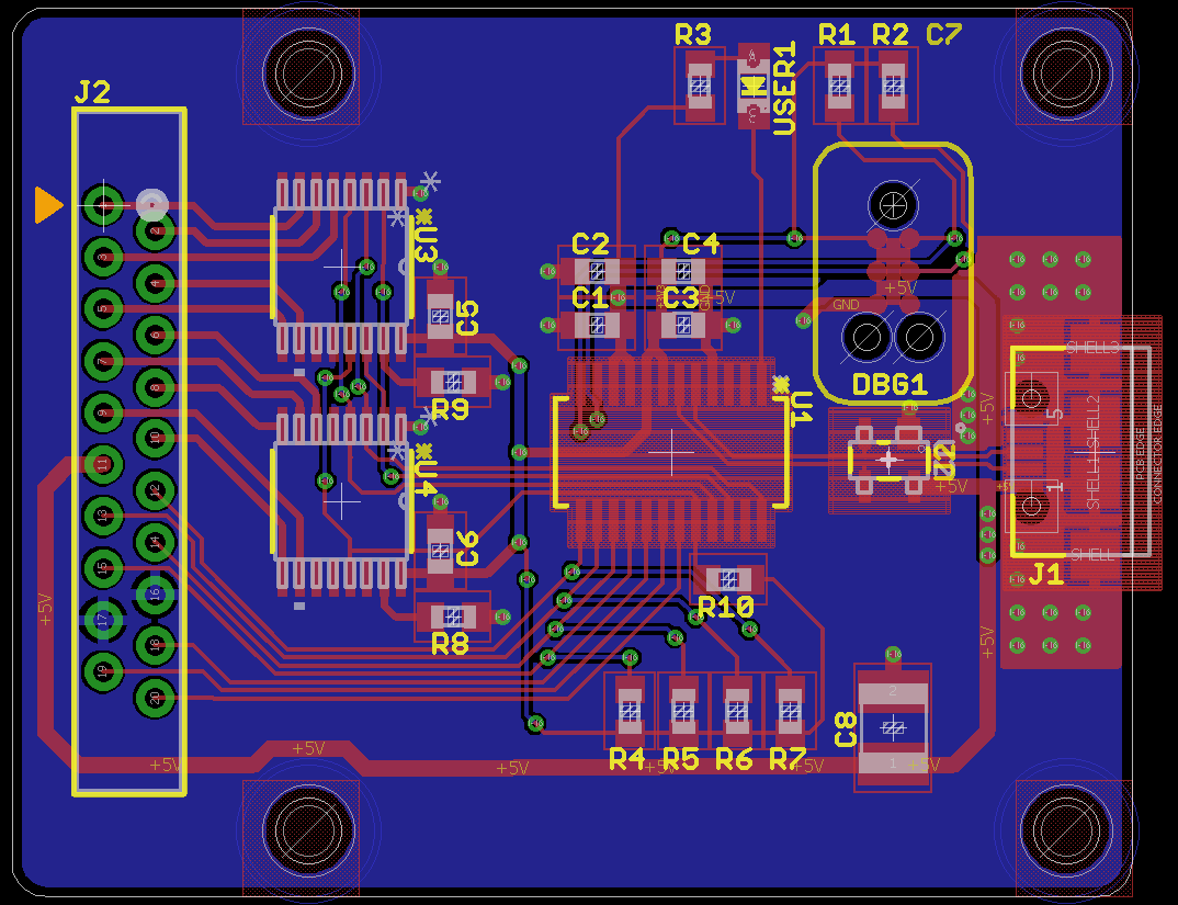
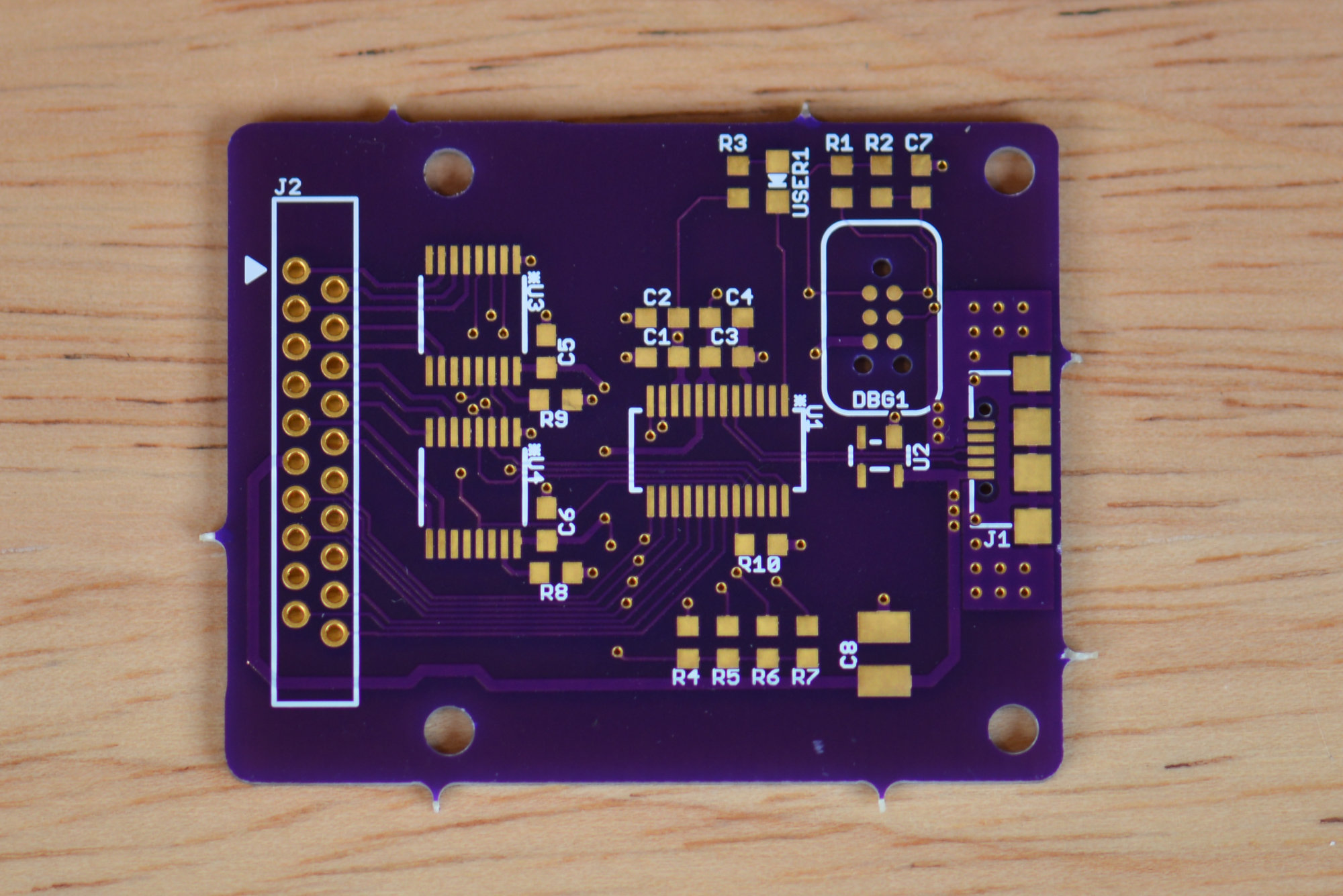
USB interface board layout for the user definable switches panel.
The board design is straight forward. The USB D+/D- data lines are kept short and as parallel to each other as possible. The four required decoupling caps for the EFMUB1 are placed within millimeters of the microcontroller. The bottom of the board contains a filled ground plane and the top of the board contains routed 3.3V and 5V power traces.
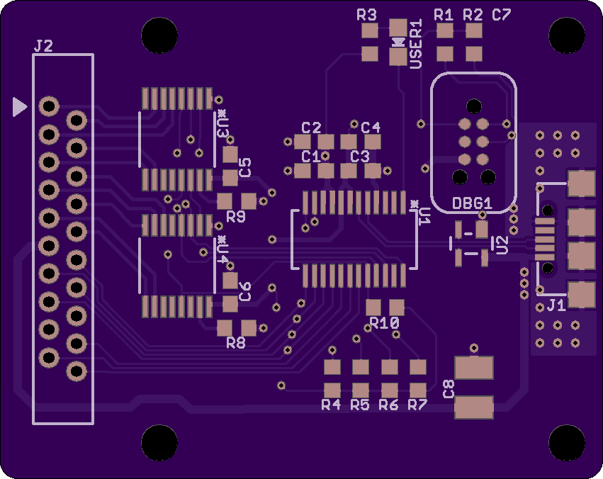
OSH Park board preview.
As usual, I uploaded the completed Gerbers to OSH Park for a preview of the manufactured board. The top of the board is shown above.
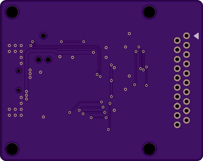
OSH Park board preview.
And the preview of the bottom side of the board.
The unstuffed board back from OSH Park.
Above is the fabricated board received back from OSH Park.
Assembling the Board
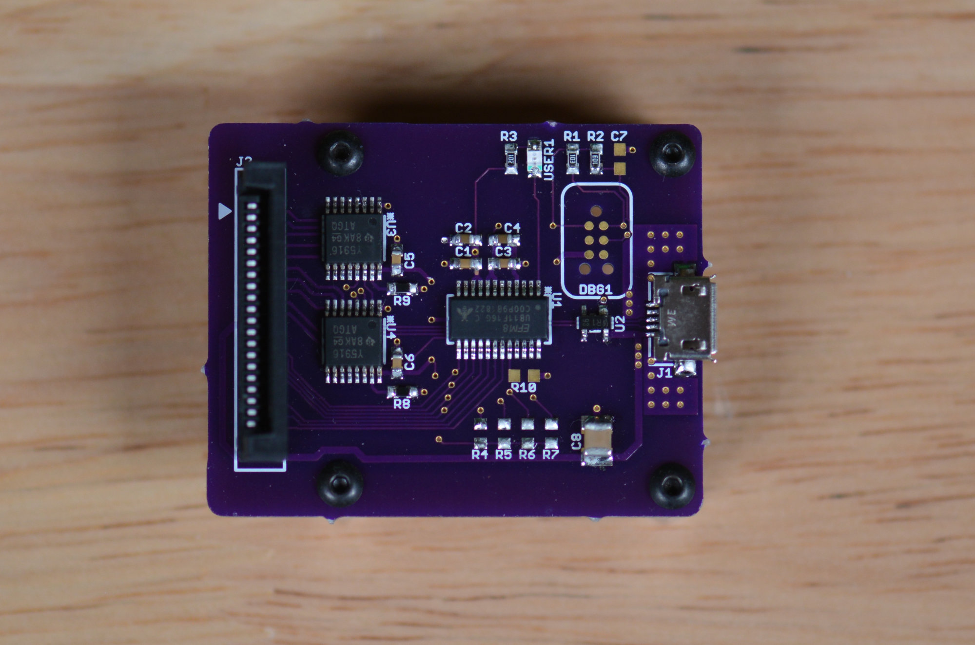
My assembled USB controller for the user definable switches panel.
Once the boards arrived from OSH Park, I hand assembled the board. This photograph is of an earlier revision of the board. C7 is gone, R10 is fixed, and R4-R7 should not have been stuffed.
EFM8UB1 Software
For software development, I started with the USB keyboard and SPI examples for the EFM8UB1-SLSTK2000A eval board. Once I was familiar with these examples, I created a new project using the hardware configurator that had the USB and SPI and their required support peripherals enabled. I then modified the generated code as needed to support a vendor-defined USB device and pasted in the SPI code from the provided examples. I also added code for a timer.
Vendor-Defined USB Device
The files descriptors.h, config/usbconfig.h, and descriptors.c contain the bulk of the code that needs to be modified to create a vendor-defined USB device. The two header files are used to set the USB vendor ID, USB product ID, number and types of USB endpoints, and enable/disable various USB options like bus-powered vs self-powered, sleep/wake, power saving modes, etc.
The descriptors.c file needs to be modified extensively to create a vendor-defined USB device. I had to add an endpoint OUT descriptor, change the interface protocol to vendor defined, and create a report descriptor describing the OUT report used to set the LEDs and the IN report used to send key presses back to the USB host.
Here’s the final report descriptor with one OUT report and one IN report:
// report 1: set lamps, 2 bytes
// report 2: get keyboard keys, 3 bytes

// HID Report Descriptor for Interface 0
SI_SEGMENT_VARIABLE(ReportDescriptor0[38],
        const uint8_t,
        SI_SEG_CODE) =
{

        0x06, 0x00, 0xFF,  // Usage Page (Vendor Defined 0xFF00)
        0x09, 0x01,        // Usage (0x01)
        0xA1, 0x01,        // Collection (Application)

        0x85, 0x01,        //   Report ID (1)
        0x95, 0x02,        //   Report Count (2)
        0x75, 0x08,        //   Report Size (8)
        0x26, 0xFF, 0x00,  //   Logical Maximum (255)
        0x15, 0x00,        //   Logical Minimum (0)
        0x09, 0x01,        //   Usage (0x01)
        0x91, 0x02,        //   Output (Data,Var,Abs,No Wrap,Linear,Preferred State,No Null Position,Non-volatile)

        0x85, 0x02,        //   Report ID (2)
        0x95, 0x03,        //   Report Count (3)
        0x75, 0x08,        //   Report Size (8)
        0x26, 0xFF, 0x00,  //   Logical Maximum (255)
        0x15, 0x00,        //   Logical Minimum (0)
        0x09, 0x01,        //   Usage (0x01)
        0x81, 0x02,        //   Input (Data,Var,Abs,No Wrap,Linear,Preferred State,No Null Position)

        0xC0,              // End Collection

        // 38 bytes
};
The OUT report is two reports of eight bits each, aka two bytes. It’s used to set the LEDs on the button panel. Each LED is set on or off based on the state of a bit in the OUT report. Which bits are mapped to which LEDs is discussed below in the “Controlling the LEDs” section.
The IN report is three reports of eight bits each, aka three bytes. It’s used to send key presses and key releases from the button panel back to the USB host. Each byte contains the state of the column signals for one row of keys. IN reports are only sent when the state of the keys changes. The mapping of keys to bits is discussed below in the “Scanning the Keypad” section.
Technically, the USB reports could be made more descriptive by using the correct fields for bits that are not used, but this is easier to make running changes to as you’re figuring out the code.
Scanning the Keypad
I decided to scan the keypad inside the USB start of frame callback. This function is called once per millisecond when the USB device, that’s us, receives a SOF packet from the USB host, that’s the Linux box/PC. The code is shown below:
uint8_t keyReportNeeded = 0;
uint8_t keyScanState = 0;
uint8_t xdata thisKeyScan[3];
uint8_t xdata lastKeyScan[3];

void USBD_SofCb (uint16_t sofNr)
{
    uint8_t i;

    UNREFERENCED_ARGUMENT(sofNr);

    idleTimerTick();

    if (!keyReportNeeded) {
        if (keyScanState < 6) {
            if (!(keyScanState & 1)) {
                // set row bits low one at a time
                P1 |= 0x07;
                P1 &= ~(1 << (keyScanState >> 1));
            } else {
                // read column inputs
                thisKeyScan[keyScanState >> 1] = (~P1 & 0x78) >> 3;
            }
            keyScanState++;
        } else {
            P1 |= 0x07;
            for (i = 0; i < 3; i++) {
                if (thisKeyScan[i] != lastKeyScan[i]) {
                    keyReportNeeded = true;
                }
                lastKeyScan[i] = thisKeyScan[i];
            }
            keyScanState = 0;
        }
    }

    // Check if the device should send a report
    if (isIdleTimerExpired() == true) {
        if (USBD_EpIsBusy(EP1IN) == false) {
            if (keyReportNeeded) {
                txBuffer[0] = 0x02;
                txBuffer[1] = thisKeyScan[0];
                txBuffer[2] = thisKeyScan[1];
                txBuffer[3] = thisKeyScan[2];
                USBD_Write (EP1IN, txBuffer, 4, false);
                keyReportNeeded = false;
            }
        }
    }
}
Two variables keep track of what state the key scanning code is in, keyReportNeeded and keyScanState. keyReportNeeded is set at the completion of a scan of the keyboard matrix if the state of the keys have changed since the last report. keyReportNeeded is cleared once a key report has been sent to the USB host. keyScanState is used to set the row key matrix rows low one at a time in succession and determine when to sample the key matrix columns.
On the first call, keyReportNeeded and keyScanState are both zero. This cause the code at the head of the callback function to cycle through each of the rows and sample the key matrix column inputs. The active row is set low while the remaining rows are left to float high. On the next call of the callback, the column inputs are sampled, inverted so a set bit indicates a pressed key, and stored in the thisKeyScanState variable.
The columns are sampled on the next call because it takes a few microseconds for the inactive rows to float back high again. This prevents sampling two rows at once. Once all the rows are scanned, thisKeyScan contains three bytes of data corresponding to the state of the column inputs for each row in the key matrix. If these three bytes differ from the last time through the scanning code, the keyReportNeeded variable is set.
When keyReportNeeded is set, the latter portion of the code waits for the idle timer to timeout, waits for IN endpoint 0 to be free, then sends the new key matrix state from thisKeyScan to the USB host. Once it’s been sent, keyReportNeeded is cleared and the process repeats.
The IN report number and three bytes of key scan data are sent to the USB host. The mapping of bits in the three bytes to key is as follows:
SW1:  00 00 08
SW2:  00 00 04
SW3:  00 00 02
SW4:  00 00 01
SW5:  00 08 00
SW6:  00 04 00
SW7:  00 02 00
SW8:  00 01 00
SW9:  08 00 00
SW10: 04 00 00
Controlling the LEDs
Controlling the LEDs is simpler than scanning the key matrix. This code resides in the transfer complete callback. This callback is called whenever a USB transfer completes on any endpoint in any direction. The code is shown below:
uint16_t USBD_XferCompleteCb(uint8_t epAddr, USB_Status_TypeDef status,
        uint16_t xferred, uint16_t remaining)
{
    uint16_t leds;

    UNREFERENCED_ARGUMENT(status);
    UNREFERENCED_ARGUMENT(xferred);
    UNREFERENCED_ARGUMENT(remaining);

    if (epAddr == EP1OUT) {
        // report 1 is  bytes, set leds
        if (rxBuffer[0] == 0x01) {
            leds = (rxBuffer[1] << 8) | rxBuffer[2];
            WriteLEDs (leds);
        }
        USBD_Read (EP1OUT, rxBuffer, 64, true);
    }

    return 0;
}
If the endpoint is out endpoint 0 and the report ID is 1, the two byte report payload is sent to the TLC5916 drivers to control the LEDs using the SPI bus. This code runs at interrupt time so the SPI bus needs to be reserved exclusively for use at interrupt time. For an example of sharing the SPI bus between mainline code and interrupt code, see the code for the USB analog panel metes project.
The first byte of the report payload is sent first on the SPI bus. This data will be shifted into the first TLC5916, U3. When the second byte of the payload is sent, the first byte will then shift out of the first TLC5916 and into the second TLC5916, U4, and the second byte of the payload will be shifted into the first TLC5916.
In other words, when the SPI transfer is complete, the first TLC5916, U3, will contain the contents of rxBuffer[2] and the sccond TLC5916, U4, will contain the contents of rxBuffer[1]. When the latch enable signal is brought high then back low again, the contents of the shift registers will be transferred to the output latch registers and the LEDs will be updated to reflect the new values.
The mapping of report payload bits to LEDs is as follows:
0x00 0x04 SW1  U3 OUT2 // First TLC5916 is chain controlled using second byte of payload
0x00 0x02 SW2  U3 OUT1
0x00 0x01 SW3  U3 OUT0
0x00 0x20 SW4  U3 OUT5
0x00 0x10 SW5  U3 OUT4
0x02 0x00 SW6  U4 OUT1 // Second TLC5916 in chain is controlled using first byte of payload
0x04 0x00 SW7  U4 OUT2
0x08 0x00 SW8  U4 OUT3
0x20 0x00 SW9  U4 OUT5
0x10 0x00 SW10 U4 OUT4
Other Code
The main loop also contains some other code. At reset, all the button panel LEDs are turned off. Timer 2 is used to create a 100 Hz tick that runs various background tasks in the main loop. One of the background tasks is to blink the USER1 LED on my PCB. This code base is older than the panel meters code base so the LED blinks at a fixed rate regardless of whether the device is enumerated on the USB bus.
Linux USB HIDRaw Software
I tested the USB code using the Linux USB HIDRaw libraries.
UDEV Permissions
The first step is to make the analog panel meter controller available to non-root users by adding a .rules file to /etc/udev/rules.d. I called my file 46-hidraw.rules. Owner and group are root with 644 permissions. To this file, I added following lines:
#EFM8 USB Custom HID Device - EFM8UB1 User Definable Switches Panel
ATTRS{idProduct}=="0006", ATTRS{idVendor}=="4247", MODE="666", GROUP="plugdev"
The new rules will take effect the next time the USB device is enumerated. Disconnecting and re-connecting the analog panel meters controller is an easy way to force an enumeration.
HIDRaw Code
I based my HIDRaw code on the HIDRaw example at https://github.com/torvalds/linux/blob/master/samples/hidraw/hid-example.c.
The first step is to open the hidraw device:
fd = open(device, O_RDWR|O_NONBLOCK);
I assume there’s only one hidraw device on the system at /dev/hidraw0. A better way would be to use the udev libraries to search for analog panel meter controllers by vendor and product ID then possibly serial number to locate a specific analog panel meters controller.
Sending OUT Reports to Control the LEDs
uint16_t leds[10] = {
    0x0004, 0x0002, 0x0001, 0x0020, 0x0010,
    0x0200, 0x0400, 0x0800, 0x2000, 0x1000
};

while (1) {
    for (i = 0; i < 10; i++) {
        buf[0] = 0x01;
        buf[1] = leds[i] >> 8;
        buf[2] = leds[i];
        write (fd, buf, 3);
        sleep (1);
    }
}
Once the hidraw device is open, controlling the LEDs in the push buttons just requires using a write call to send three bytes to the controller. The first byte is the output report ID (0x01). The next two bytes contain a bitmap to turn individual LEDs on or off. The example code above cycles through the ten LEDs on the panel in sequence pausing for one second between LEDs.
Receiving IN Reports with Key Presses
while (1) {
    count = read (fd, buf, 4);
    if (count > 0) {
        for (j = 0; j < count ; j++) {
            printf("%02x ", buf[j] & 0xff);
        }
        printf("\n");
    }
    usleep (50000);
}
Reading the keys is slightly more complicated than controlling the LEDs. To read the keys, call read with the previously opened file descriptor and a buffer with a size of at least four. Since we opened the file descriptor with the O_NONBLOCK, the read call will returne immediately. If data is available to be read, the return value will indicate the number of bytes available. The example code above reads the key presses then displays the report ID and three bytes of keypress data on the screen. The usleep call is to prevent a busy wait from hogging the CPU.
Here’s the output of the above code when pressing the keys in sequence from left to right:
02 00 00 08 // SW1 down
02 00 00 00
02 00 00 04 // SW2 down
02 00 00 00
02 00 00 02 // SW3 down
02 00 00 00
02 00 00 01 // SW4 down
02 00 00 00
02 00 08 00 // SW5 down
02 00 00 00
02 00 04 00 // SW6 down
02 00 00 00
02 00 02 00 // SW7 down
02 00 00 00
02 00 01 00 // SW8 down
02 00 00 00
02 08 00 00 // SW9 down
02 00 00 00
02 04 00 00 // SW10 down
02 00 00 00
Next Steps
Finding parts and pieces of a video switcher is a pretty rare occurrence. This project could be built using any off the shelf keypad or even building your own keypad. Another project idea would be to modify the software to create a combined HID keyboard and HID vendor-defined device. The keys could activate macros while the user’s software could activate the LEDs as needed.
Bill of Materials
The bill of materials is listed below.
| Qty | Parts | Description | Mfr | Mfr Part # | Dist | Dist Part # |
| 11 | C1,C3,C5,C6 | CAP CER 0.1UF 50V X7R 0603 | KEMET | C0603C104K5RACTU | Digi-Key | 399-5089-1-ND |
| 2 | C2, C4 | CAP CER 1UF 16V X7R 0603 | KEMET | C0603C105K4RACTU | Digi-Key | 399-7847-1-ND |
| 1 | C8 | CAP CER 1UF 25V X7R 1210 | KEMET | C1210C105K3RACTU | Digi-Key | 399-8220-1-ND |
| 1 | J1 | CONN RCPT USB2.0 MICRO B SMD R/A | Würth Elektronik | 629105136821 | Digi-Key | 732-3155-1-ND |
| 1 | J2 | CONN FFC FPC VERT 20POS 1MM PCB | Amphenol ICC (FCI) | SLW20S-1C7LF | Digi-Key | 609-1949-ND |
| 7 | R1, R2, R4, R5, R6, R7, R10 | RES SMD 10K OHM 5% 1/10W 0603 | Panasonic Electronic Components | ERJ-3GEYJ103V | Digi-Key | P10KGCT-ND |
| 1 | R3 | RES SMD 1K OHM 5% 1/10W 0603 | Panasonic Electronic Components | ERJ-3GEYJ102V | Digi-Key | P1.0KGCT-ND |
| 2 | R8, R9 | RES SMD 1.2K OHM 5% 1/10W 0603 | Panasonic Electronic Components | ERJ-3GEYJ122V | Digi-Key | P1.2KGCT-ND |
| 1 | U1 | IC MCU 8BIT 16KB FLASH 24QSOP | Silicon Labs | EFM8UB11F16G-C-QSOP24 | Digi-Key | 336-3411-5-ND |
| 1 | U2 | TVS DIODE 5.5V SOT143B | Nexperia USA Inc. | PRTR5V0U2X,215 | Digi-Key | 1727-3884-1-ND |
| 2 | U3, U4 | IC LED DRIVER LIN 120MA 16TSSOP | Texas Instruments | TLC5916IPWR | Digi-Key | 296-22711-1-ND |
| 1 | D1 | LED GREEN CLEAR CHIP SMD | Kingbright | APHCM2012CGCK-F01 | Digi-Key | 754-1094-1-ND |
Design Files
Design files for this project are in my usb-led-switch-matrix repository on GitHub.