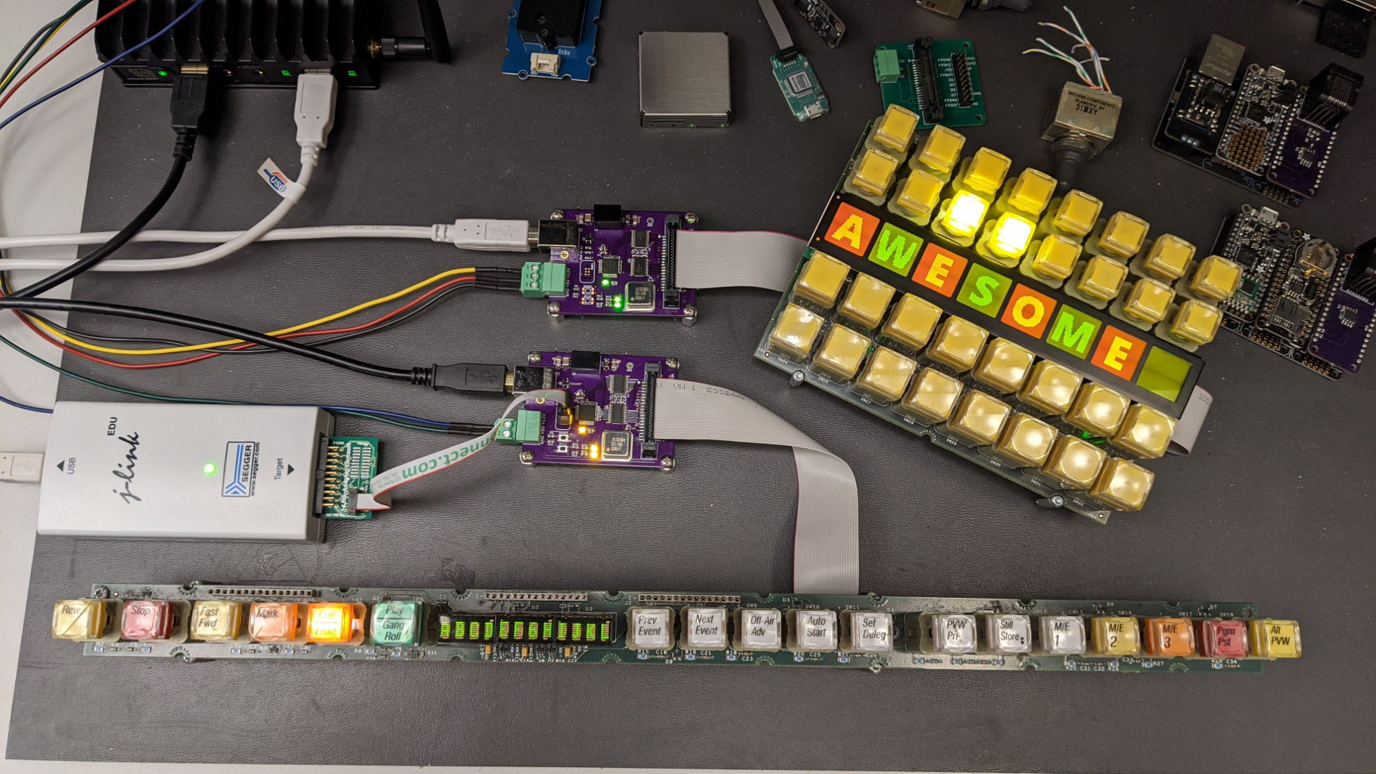
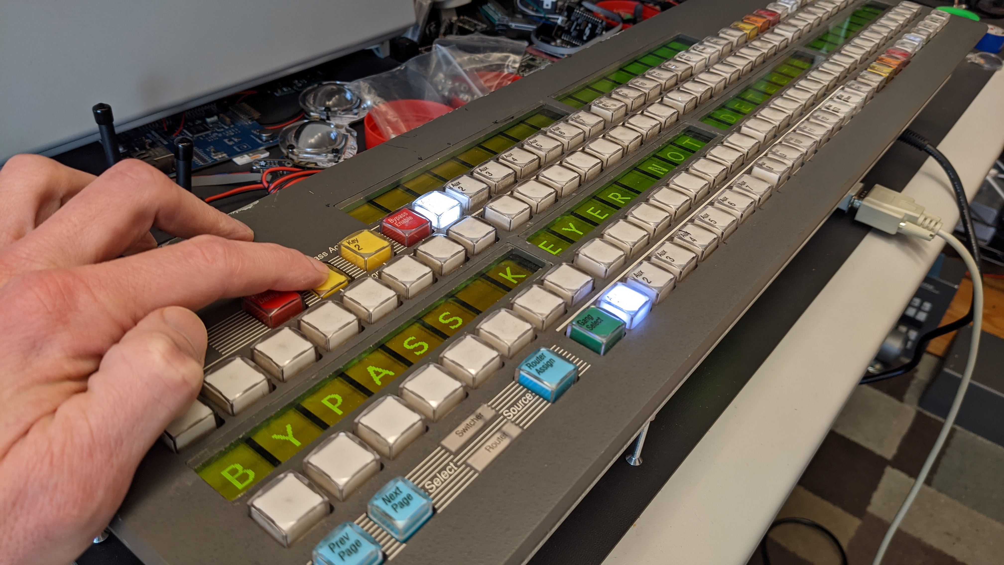
A Grass Valley Kalypso video switcher machine control panel (bottom) and crosspoint switch panel (upper right) after converting them into USB human interface devices using Silicon Labs EFM8UB2 USB microcontrollers.
In this project, I convert two panels from a vintage Grass Valley video switcher into general-purpose USB input and output devices without modifying the original panels. This project required both reverse engineering the hardware and deciphering the software protocols used to communicate with the panels. Because these panels required learning how to communicate with a microcontroller and a small FPGA, this project was significantly more challenging than the previous project where I converted a matrix button panel from the same mixer into a USB device.
In this write up, we’ll examine the two panels in detail and determine the hardware interface to the panels. Once the hardware interface is determined, we’ll build some boards to use to help decipher the protocols used to control the boards. Once the protocols are understood, we’ll build a second set of boards to control the panels using USB then develop the USB software and an example Linux application that controls the panels over USB. This project took about four months from start to completion.
The Panels’ Lineage
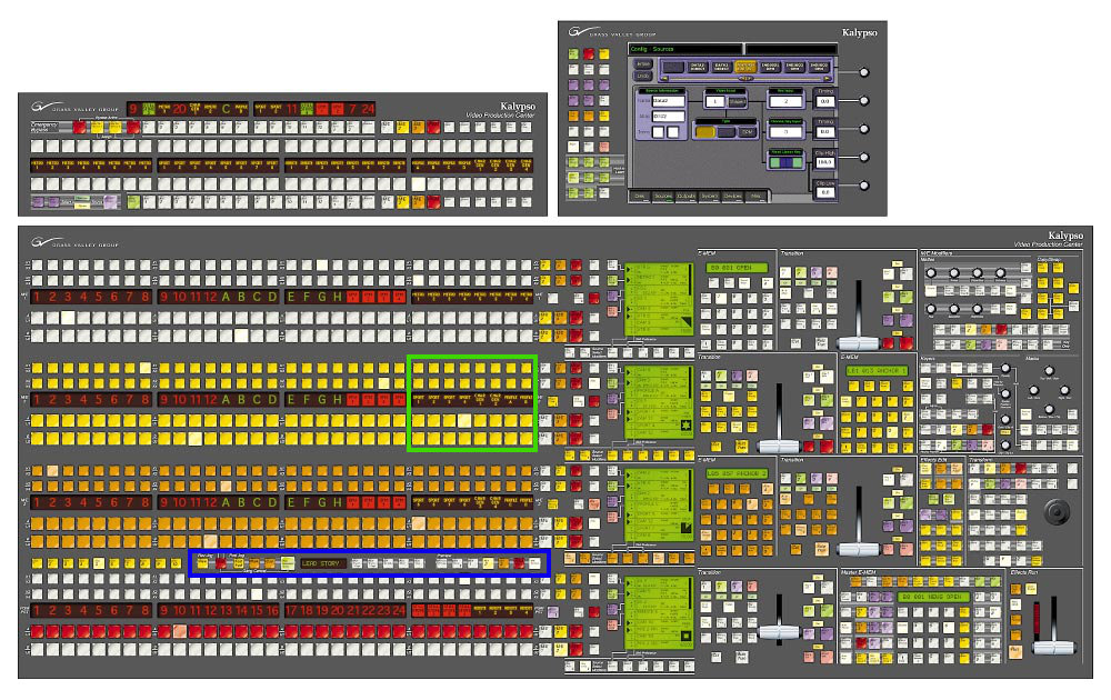
The machine control panel is circled in blue. It is immediately to the right of the user definable switches panel described in the previous blog post. One of the 16 crosspoint panels on this 4-M/E control surface is circled in green. That’s 512 buttons just for selecting sources! Image from manufacturer’s preliminary data sheet circa 2000.
In this project, I use two different panels from a Grass Valley Kalypso 4-M/E video switcher control surface. The first panel is the machine control panel, circled in blue above. The machine control panel sits immediately to the right of the user definable switches panel used for the previous project. The second panel is the crosspoint switch panel, circled in green above. Both of these panels have similar hardware and software architectures.
Machine Control Panel Overview
The machine control panel is used to control video tape recorders and video servers connected to the mixer. A typical use case might be on the local news when an anchor says something along the lines of “Tom spoke with the governor earlier today” and then the video cuts to the previously recorded interview. The machine control panel is used to select the interview, queue up the footage, then start playback. Once the footage is rolling, the crosspoint switch panel and transition panel are used to switch the footage to air.
Top
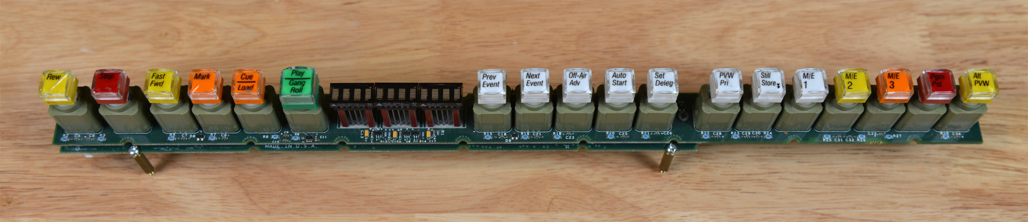
The top of the top board in the machine control panel board stack.
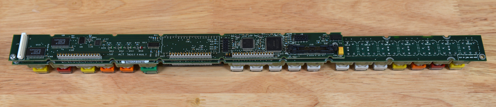
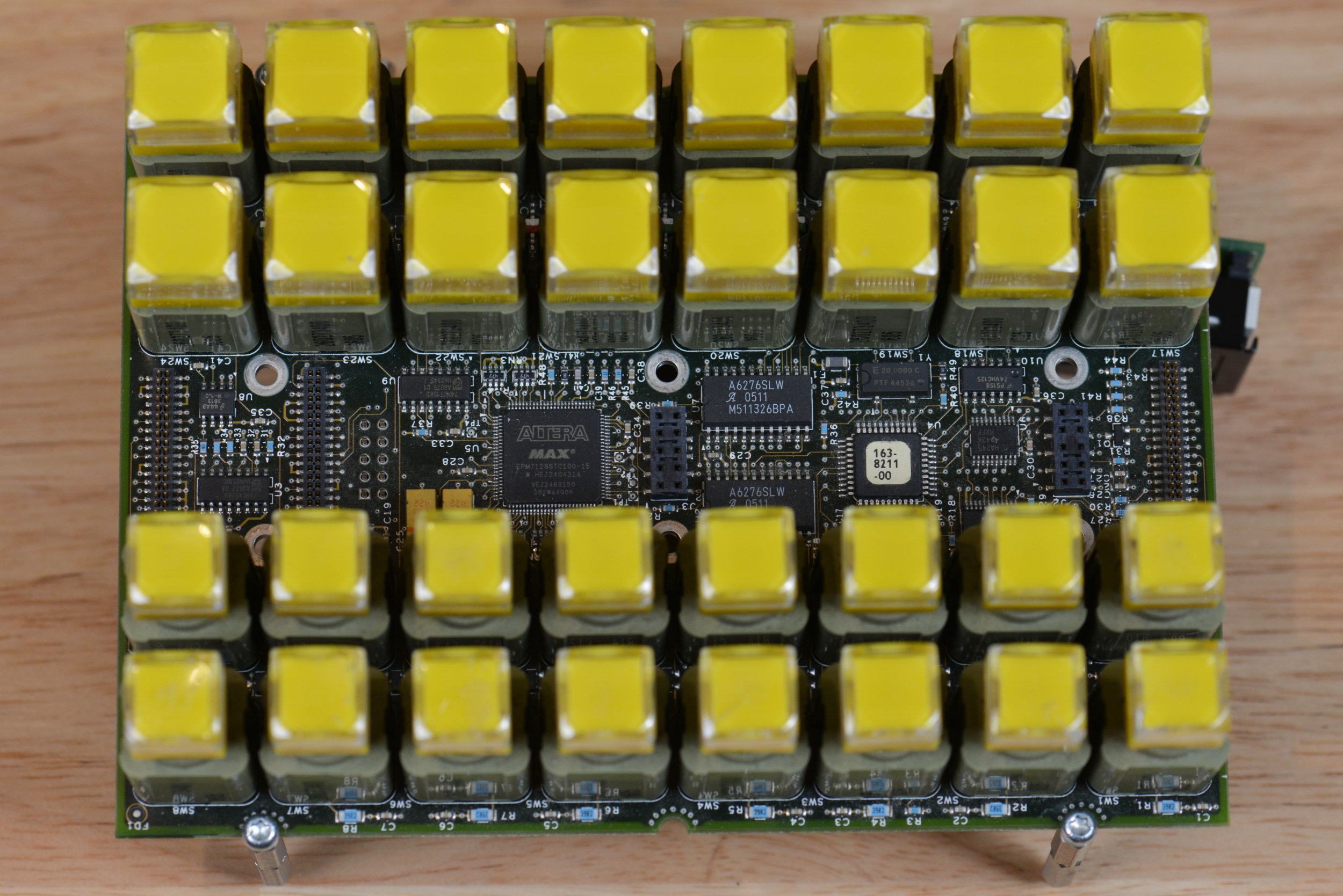
The machine control panel is a stack of two boards. The top board, seen above, contains 18 illuminated push buttons and a 12 character LED display. The bottom board contains the logic to interface the buttons and display to a single board computer in the 4-M/E control surface.
Buttons
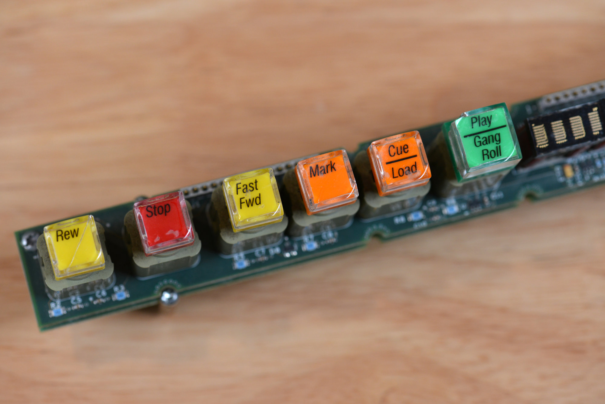
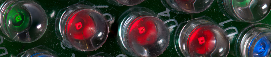
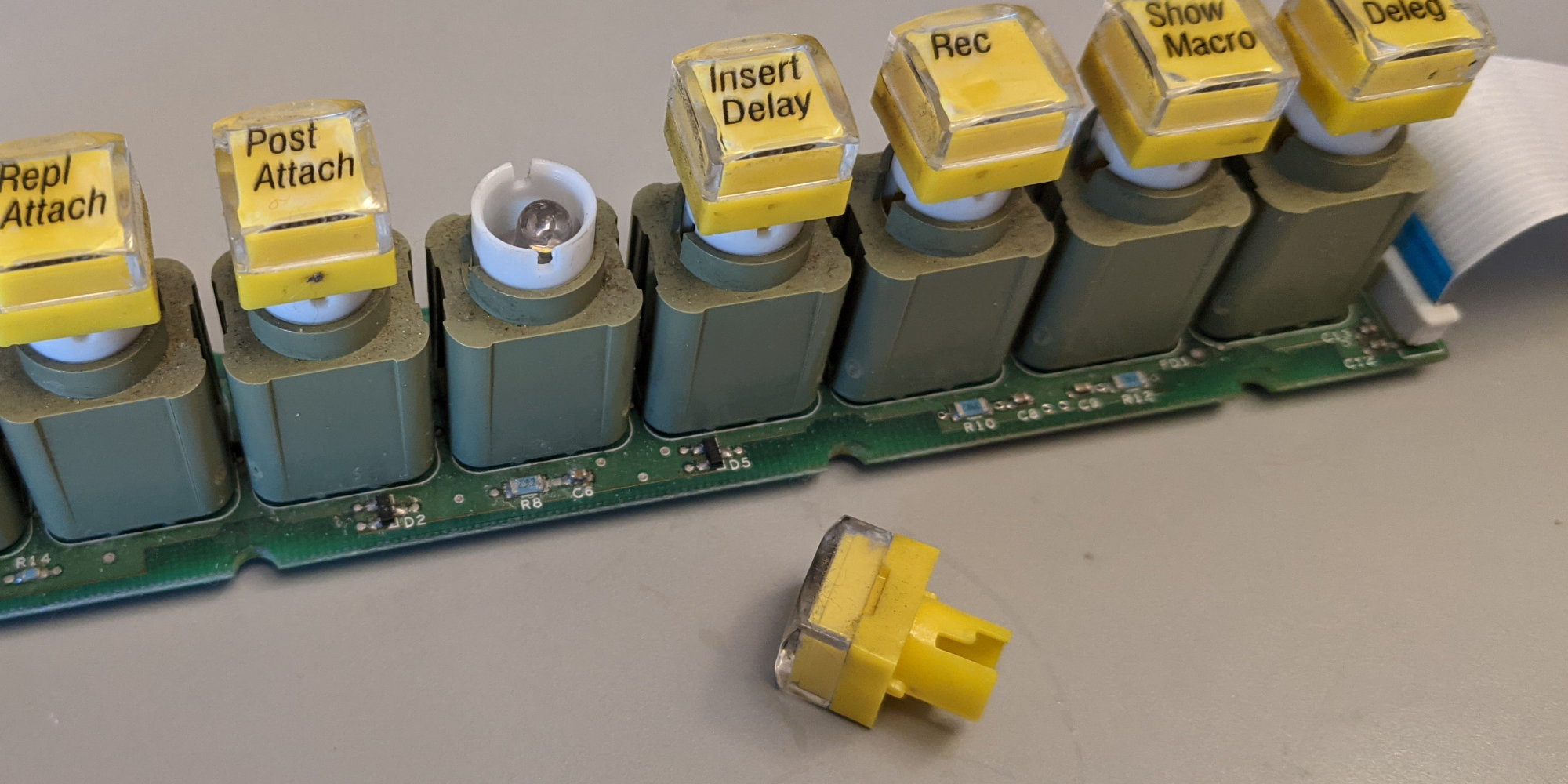
Close up of six of the 18 buttons on the machine control panel. The green play button is slightly larger than the rest of the buttons.
Like the user definable switches panel, the machine control panel uses the same fantastic Veetronix illuminated magnetic reed push button switches. There’s a total of 18 buttons in a variety of colors. The green play button’s key cap is slightly larger than the rest of the key caps. The previous post describes these switches in great detail and includes a page from their 1993 patent.
LED Display
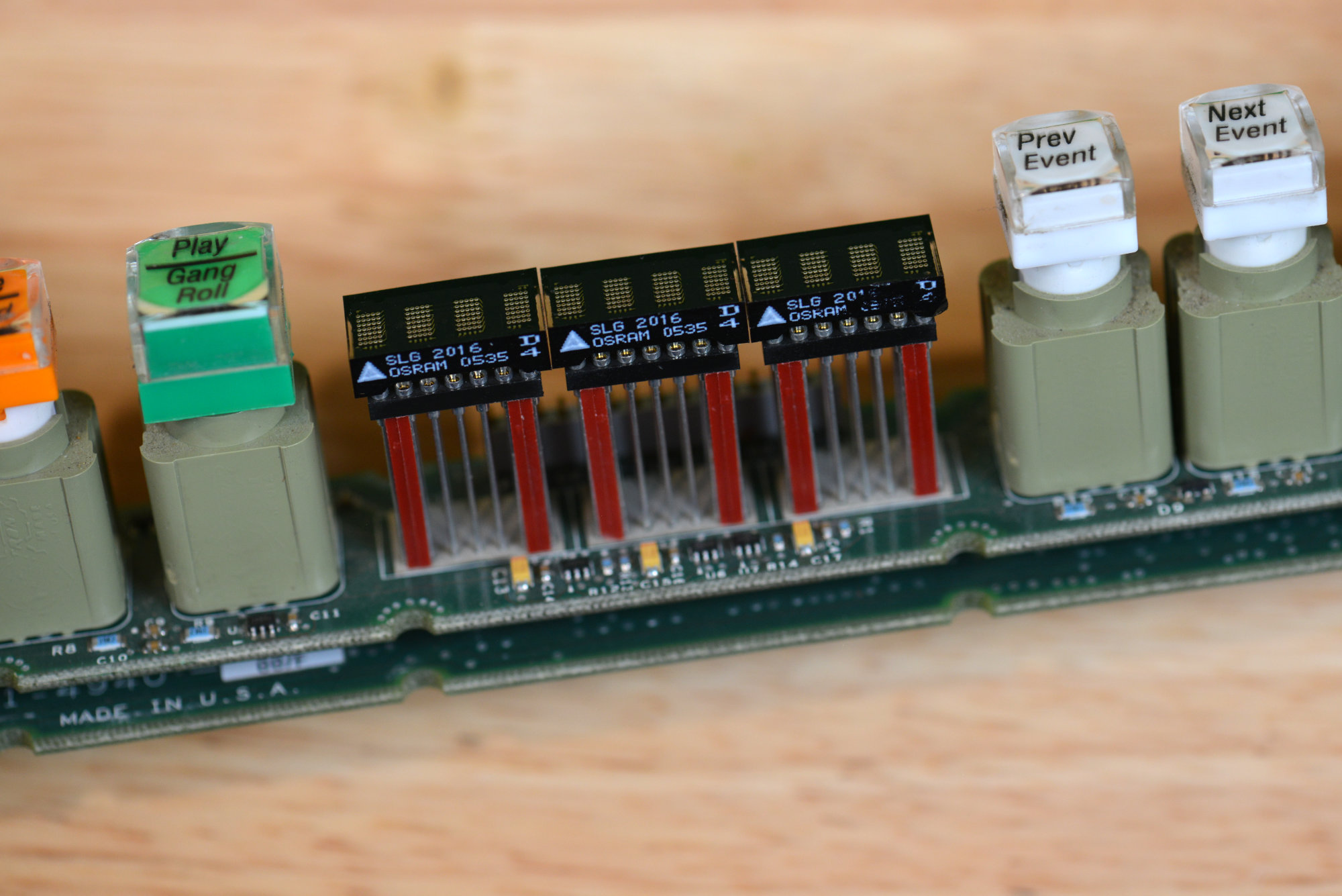
Close up of the three four-character alphanumeric displays on the machine control panel.
The machine control panel has a 12 character alphanumeric display for selecting and displaying the name of the queued clip. This display consists of three four-character OSRAM SLG2016 displays. These particular displays were manufactured in the 35th week of 2005 thus giving an approximate time frame for when this panel might have been in service.
Block diagram of the OSRAM SLG2016 LED dot matrix displays from the datasheet.
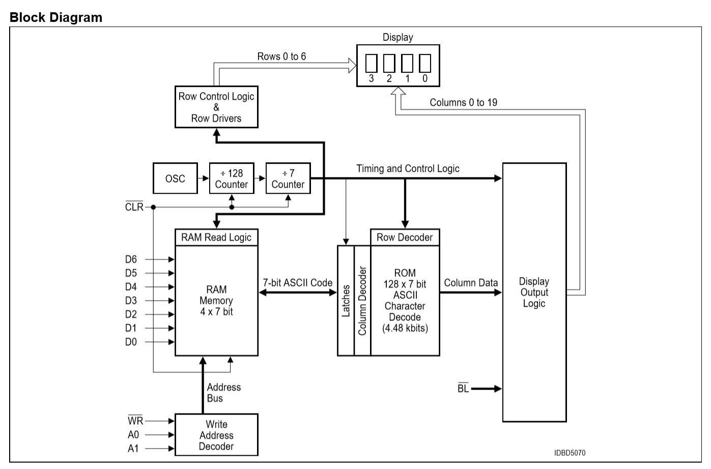
These displays are “intelligent” in that you write a character code into a RAM location in the display then the display decodes and displays the character without further intervention by the processor. Each glyph is stored in a character ROM then displayed on a multiplexed 5×7 LED matrix. The display may be dimmed by pulse-width modulating the blanking input. I do not believe the dimming feature is used on this panel.
Bottom
The bottom of the bottom board in the machine control panel board stack.
Pictured above is the bottom of the bottom board in the machine control panel’s two board stack. This board contains the logic and drivers for the buttons and display. The three gray connectors along the bottom connect the top board with the buttons and displays to the bottom board with the logic and drivers. Let’s examine the logic board in detail moving from left to right.
Mezzanine Connector and LED Drivers
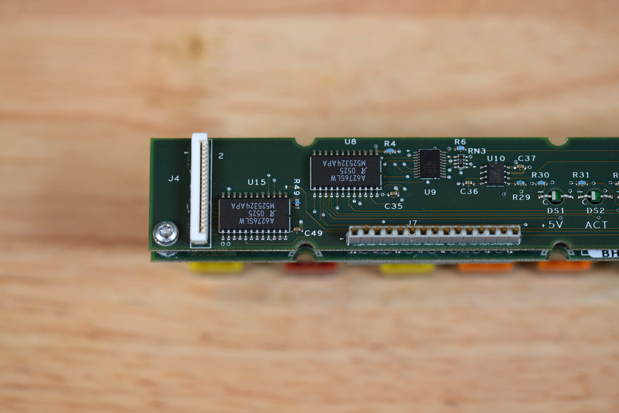
Close up of the machine control panel bottom board showing the mezzanine connector for the user definable switches panel and the A6276SLW constant-current LED driver ICs.
On the far left hand side of the logic board is the 20-pin, 1 mm pitch flex connector that connects to the user definable switches board. The machine control panel is also responsible for scanning the keys and driving the LEDs on that board.
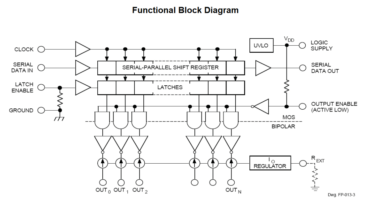
Functional block diagram from the Allegro Microsystems A6276SLW datasheet.
Immediately to the connector’s right are two Allegro Microsystems A6276SLW 16-channel, constant current LED drivers. The part has a serial peripheral bus interface and multiple parts can be daisy chained in series. The outputs of these drivers connect to the LEDs on the user definable switches panel and the machine control panel. This part is obsolete but is very similar in operation to the eight-channel Texas Instruments TLC5916 LED driver.
Diagnostic LEDs
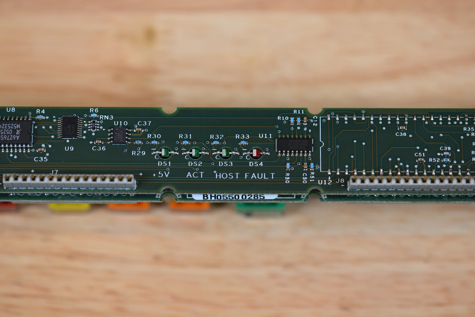
Close up of the machine control panel bottom board showing the diagnostic LEDs.
To the right of that are miscellaenous logic ICs and four diagnostic indicators, +5V, ACT, HOST, and FAULT. This is our first indication of the power supply voltage required for this board to operate.
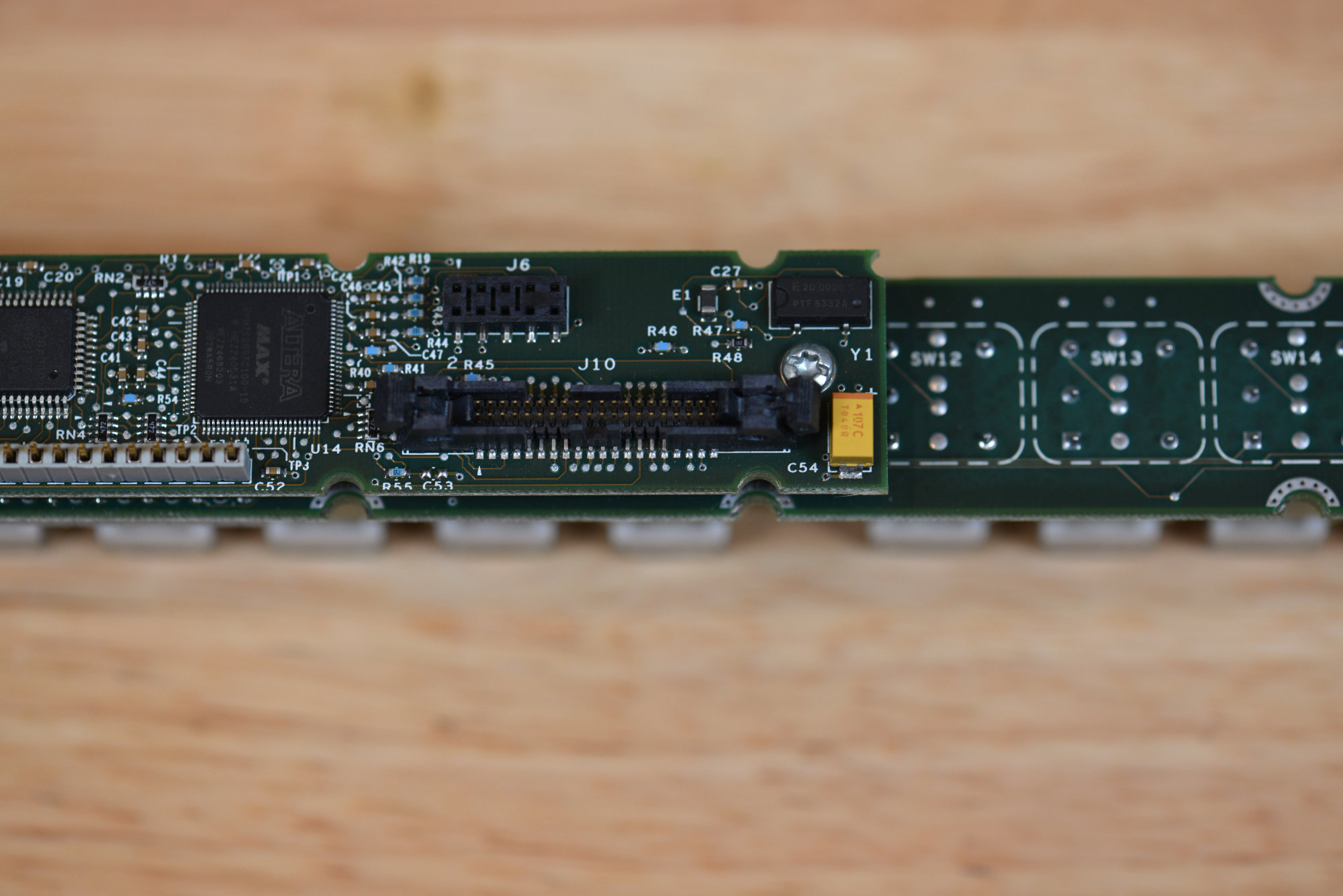
Microcontroller and FPGA
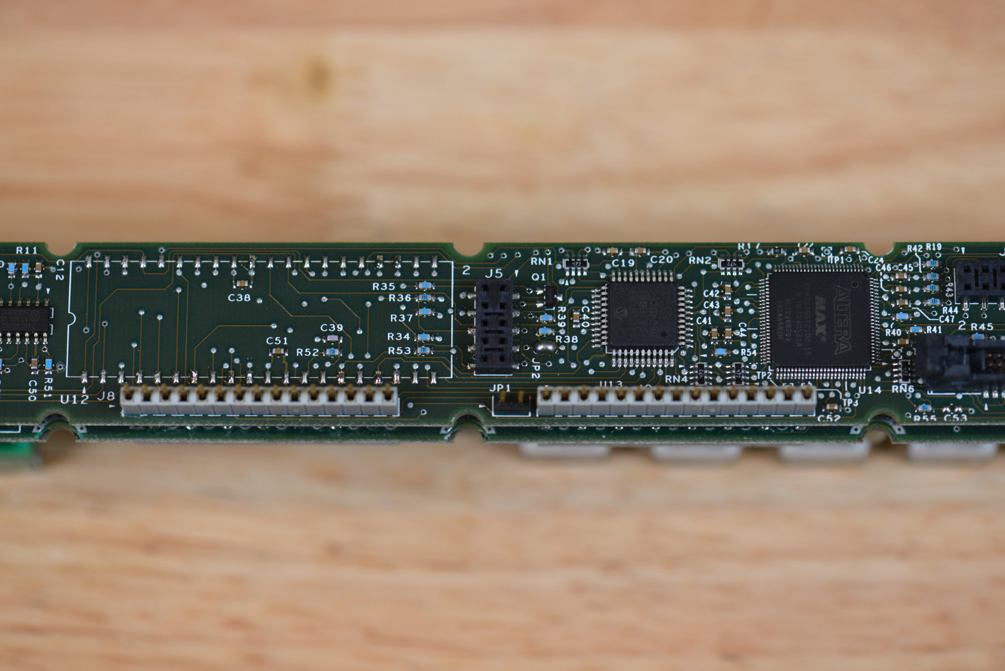
Close up of the machine control panel bottom board showing the empty pads for the PIC16C67 used for firmware devlopment, the final PIC16C67 microcontroller in a non-windowed TQFP package, and the Altera MAX PLD.
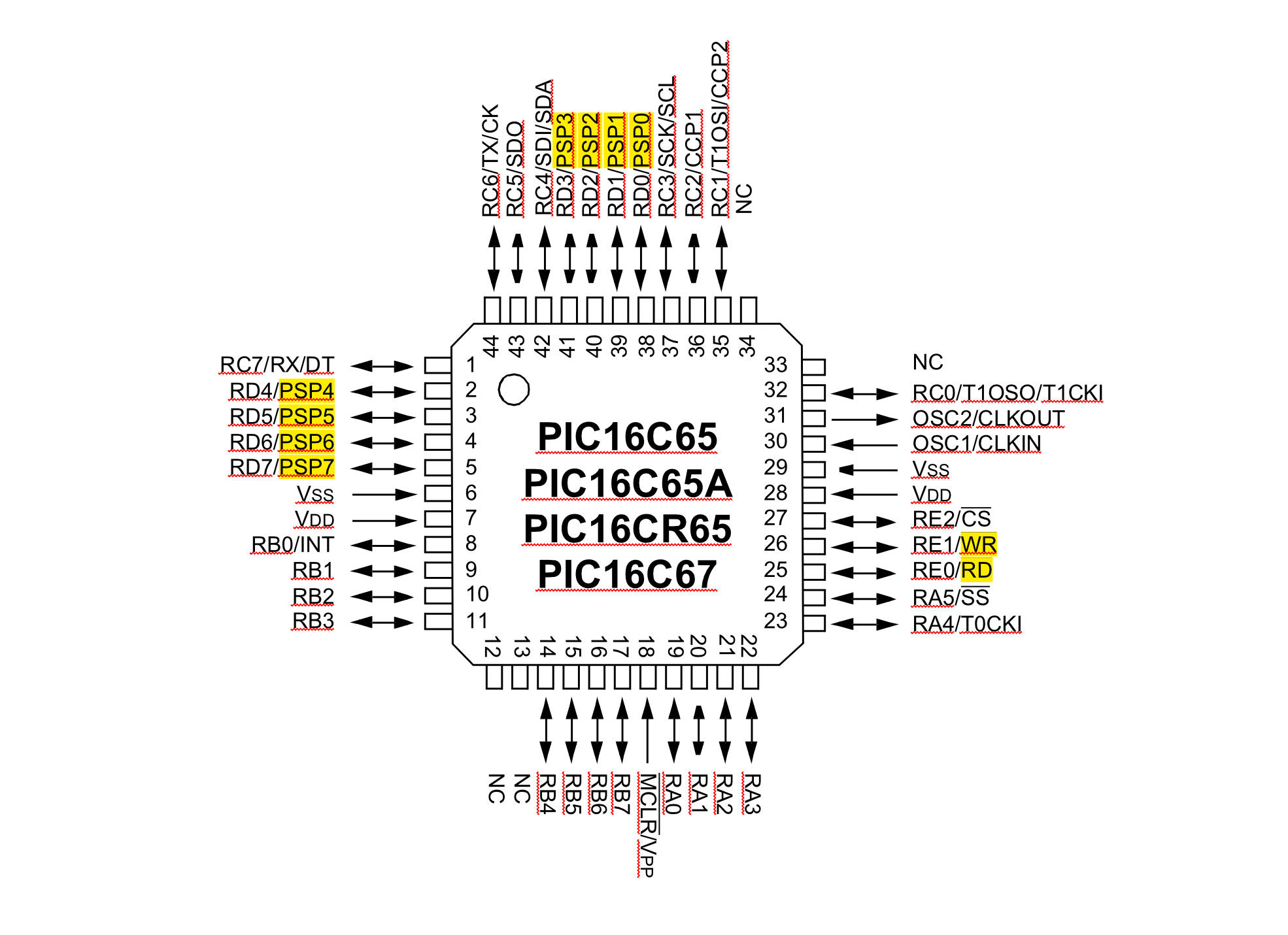
To the right of the diagnostic indicators are a PIC16C67 microcontroller and an Altera MAX EPM7128STC100-15 PLD. There are also pads for a surface mount 40-pin DIP socket that is unpopulated. The PIC and the PLD are going to cause unnecessary complications when reverse engineering this panel because I do not know what software the PIC is running or what logic is implemented in the PLD. If I can’t determine the functionality of the software and PLD logic, I may have to revert to plan B and harvest the buttons and displays for use on a board of my own design.
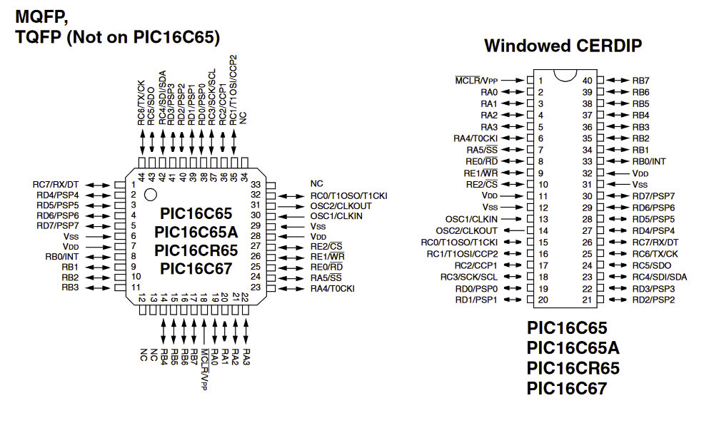
WIndowless PIC16C67 TQFP package pin out versus ceramic DIP windoweed PIC16C67 pin out from the PIC16C67 data sheet.
The PIC16C67 is an EPROM-based microcontroller. Since the TQFP package is windowless, it cannot be erased with a UV eraser and is therefore a one-time programmable (OTP) device.
To facilitate software development, the board designers included a surface mount 40-pin DIP socket footprint connected in parallel to the TQFP PIC16C67. During development, the TQFP part is not populated and a zero-insertion force (ZIF) socket is installed on the 40-pin DIP footprint. This permits windowed ceramic DIP packages to be used for software testing then removed, erased, and reused when a bug is found in the code.
Alternatively, an in-circuit emulator that plugs into the DIP socket may be used. In-circuit emulators from this era are usually big, temperamental boxes connected via a finicky ribbon cable to a giant plug with DIP pins on them. The DIP pins plug into the circuit where the microcontroller would normally be.
The in-circuit emulator contains a special version of the microcontroller that has additional pins bonded out for debug use. This is very much unlike today’s trim, modern serial-based JTAG and ARM CoreSight debuggers where the debug circuitry is included in every chip produced and a minimal number of wires to use it are bonded out on every chip produced.
There are also two 10-pin 0.1″ pitch 2×5 header sockets that are used to program the PIC and PLD once the board is manufactured. The PIC is EPROM-based and one-time programmable. The PLD is EEPROM-based and may be programmed, erased, and re-programmed as needed. Both parts are five volt devices.
Interface Connector
Close up of the machine control panel bottom board showing the 40-pin, 1.27 mm pitch connector used to connect to the single board computer in the base of the control surface.
At the far right of the board is a 40-pin, 2 row x 20 position, 1.27 mm pitch shrouded header. A cable connects from this header to the single board computer that runs the control surface. Ideally, I could connect my USB hardware to this connector to re-purpose the board. There’s also a 20 MHz oscillator that is connected to the PIC and possibly the PLD but I did not verify the PLD connection.
Crosspoint Switch Matrix Panel Overview
A Kalypso 4-M/E control surface has 16 rows of 32 columns of buttons that are used to route video sources to four mix-effects boards for processing and output to air. Each column represents a different video source. Each row represents a different input on one of the four mix-effects boards and each mix-effects board has four inputs. The rows are divided into four color-coded groups and each color coded group selects the sources fed to one mix-effects board.
Top View
My 8 in by 4 out crosspoint switch matrix panel from the M/E-2 bus on a Kalypso video switcher.
The 4 rows of 32 buttons within a color-coded mix-effects group are constructued from smaller panels of 4 rows of 8 buttons. I have one such panel from the yellow group. The yellow group is used to select up to four inputs to feed to mix-effects board 2 or “M/E 2″ as it’s labeled on other parts of the panel.
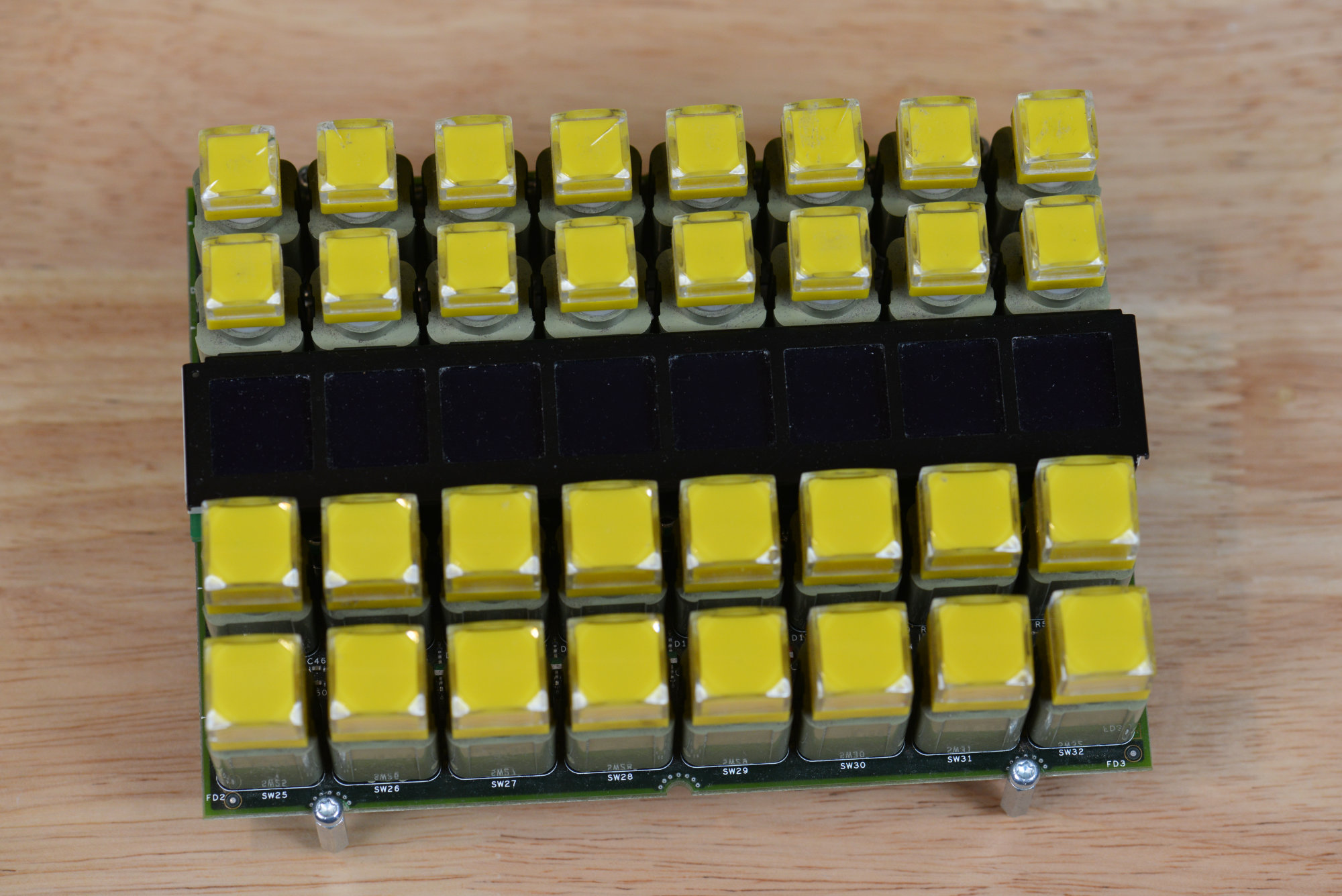
This panel has 32 Veetronix illuminated pushbuttons with yellow caps arranged in four rows of eight buttons. The top two rows have smaller caps than the bottom two rows. The top two rows are primarily used to select keys and backgrounds for effects while the bottom two rows are primarily used to select video sources for mixing and effects.
In the middle of the panel is an LCD display with eight windows built into a metal frame running the length of the panel. Grass Valley calls the LCD module the source name display because it displays the names of the video sources.
Bottom
Rear view of the crosspoint switch matrix panel.
On the bottom of the panel are two 40-pin, 1.27 mm pitch shrouded headers and a 10-pin 0.1″ pitch shrouded header. There’s also an unpopulated footprint for a 40-pin SMD DIP socket just like on the machine control panel.
The 40-pin headers connect the crosspoint switch panel to the single board computer (via a transition board as I learned later) and / or its neighboring crosspoint switch panels. The 10-pin header is used to supply power to the board since the cables used with the 1.27 mm pitch connectors cannot carry the current required to power four of these panels simultaneously.
This panel has +5V, ACTIVITY, HOST, FAULT, and +12V diagnostic indicators so it likely requires both +5V and +12V to operate.
LED Drivers, Microcontroller, FPGA, and Display Connector
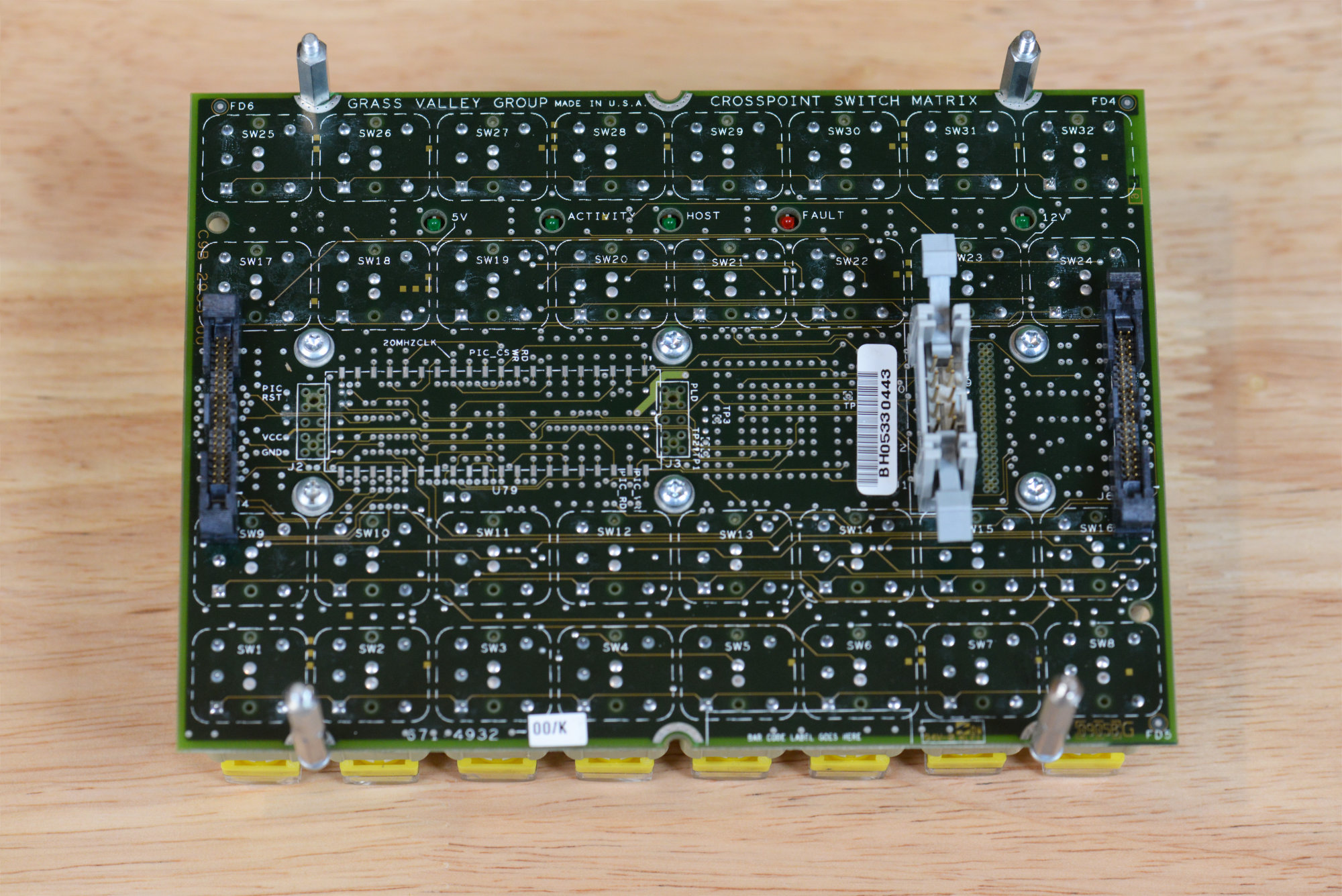
The crosspoint switch matrix panel’s circuitry is hidden underneath the source name display’s LCD module.
Removing the LCD module from the crosspoint switch panel reveals the circuitry used to scan the buttons, control the tally lights, and control the LCD. The architecture is very similar to the machine control panel’s architecture.
There’s a PIC16C67 microcontroller and an Altera MAX EPM7128STC100-15 PLD. There’s also a 20 MHz oscillator, two Allegro Microsystems A6276SLW 16-channel, constant current LED drivers, and programming connectors.
A surface mount 40-pin DIP socket footprint is wired in parallel with the PIC16C676 TQFP footprint on the reverse side of the board to permit software development using either windowed ceramic DIP packages or an in-circuit emulator.
LCD Module
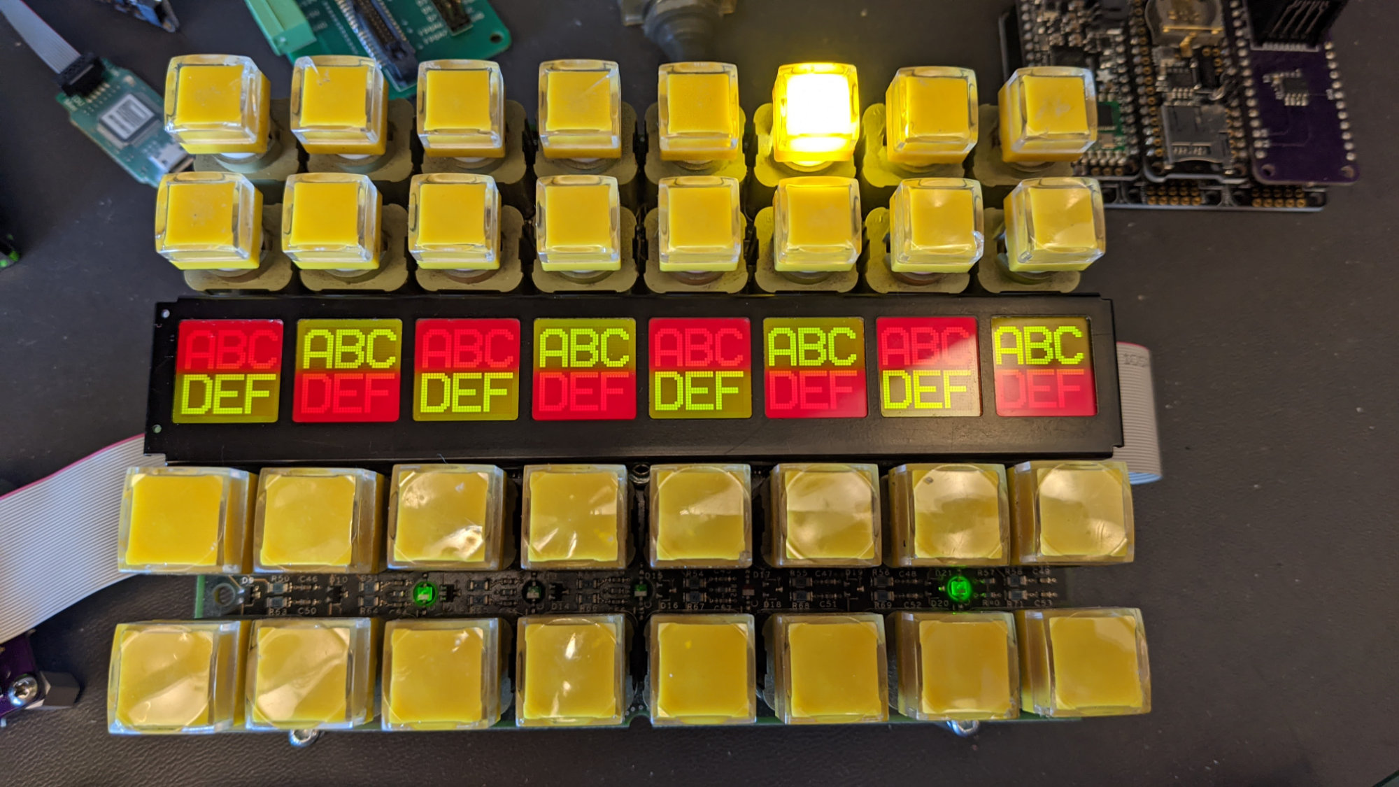
The LCD module showing the eight windows, some example text, and the split backlight.
The LCD module is super interesting and completely bespoke. It is not one long LCD panel divided up into eight windows by the frame. Instead it is eight individual 32×32 matrices on a single pane of glass and each matrix is slightly smaller than its window in the frame. This way there are no hidden pixels underneath the vertical dividers on the frame.
These 8 32×32 matrices are connected to three independent LCD controller ICs. The backlights for each window are divided into a top half and the bottom half. Each of the two halves can be set to red, green, or amber (both red and green) separately as seen in the photo above.
Board Sandwich
Side view of the LCD module.
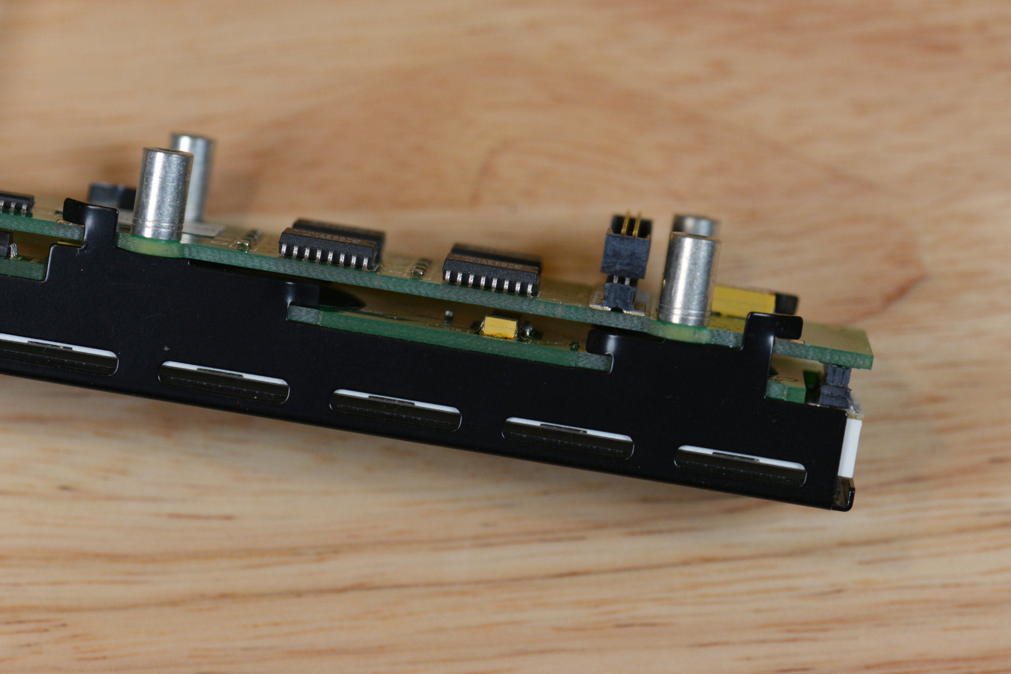
As can be seen in the side view above, the LCD module is quite complicated. It consists of a frame, a pane of glass with the matrices, a thick white 16-segment red/green/amber backlight module, a board with the three controller ICs hidden under black blobs, and a backlight control / logic board. If you look closely in the above photo, you can make out one of the black blobs on top of the middle board about an inch to the left of the yellow capacitor. The LCD controller board connects to the LCD glass using thin flexible printed circuits.
Bottom View
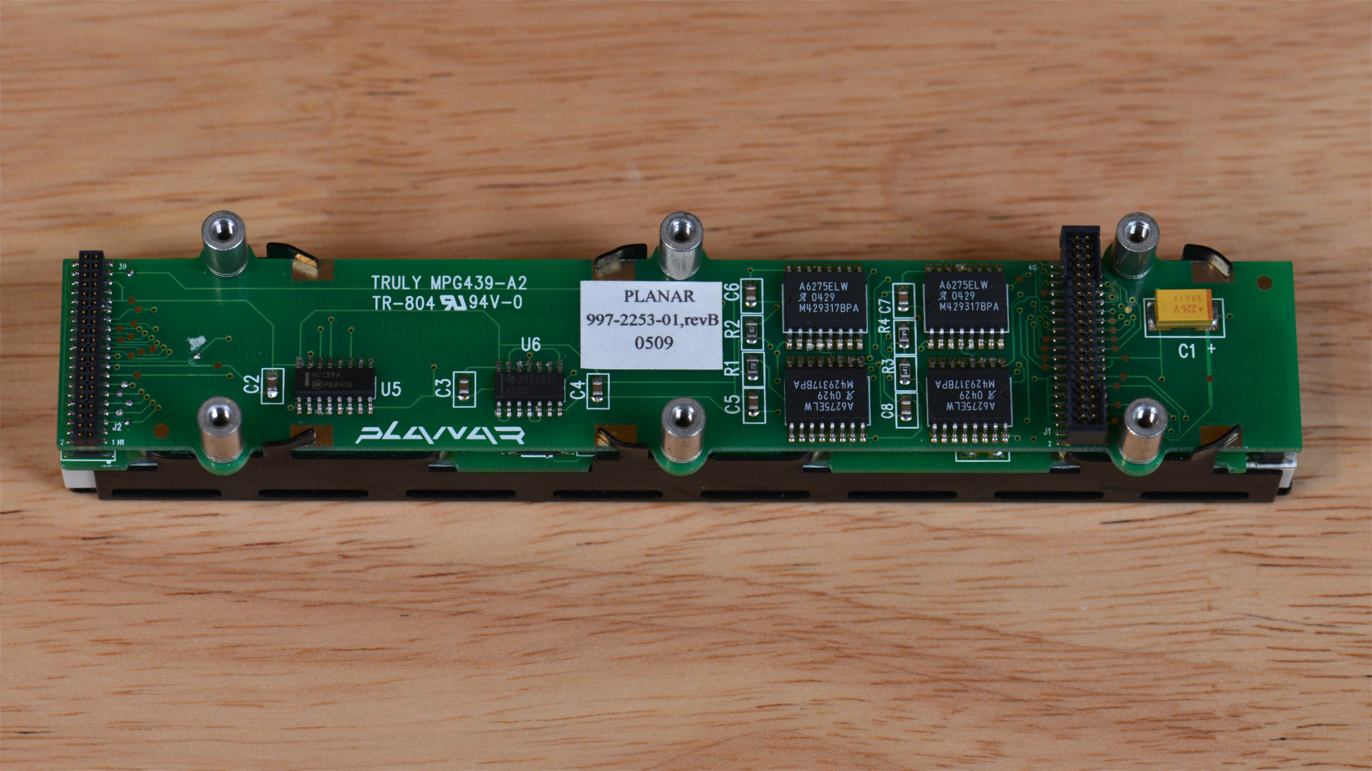
Bottom view of the LCD module.
Above is the view of the bottom of the LCD module. The LCD module connects to the crosspoint switch panel using the 40-pin, 1.27 mm pitch connector on the right hand side of board in the photo above. A similar 40-pin connector on the left hand side of the board connects this board to the board with the three LCD controllers. The LED backlights are connected to this board using a surface mount connector mounted on the reverse side of this board.
Also located on this board are four Allegro Microsystems A6276ELW eight-channel, constant-current LED drivers for the LED backlights and some glue logic that implements the LCD controller chip selects and the LED backlight clock and latch enable signals. The LCD module is held in place using six torx head screws that screw into the six standoffs shown in the photo.
Reverse Engineering the Interface Connector
After a careful examination of the hardware, I decided I wanted to try to use the boards unmodified by designing a USB controller to connect to their existing 40-pin connectors. I also decided I would be less heartbroken if I accidentally destroyed the machine control panel rather than the crosspoint switch matrix panel so I decided to start my reverse engineering efforts with the 40-pin connector on the machine control panel.
Machine Control Panel Interface Connector
There’s no easy way to do this. I got out my DMM and set it for continuity test mode and began looking for connections between the 40-pin connector and other components on the machine control panel. I started with the grounds:
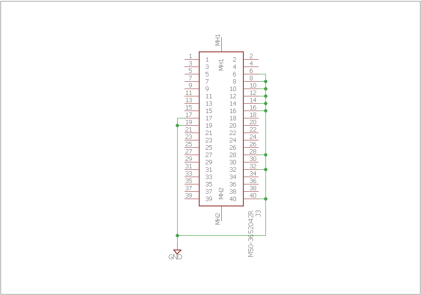
Machine control panel 40-pin connector grounds.
After finding all the grounds, I searched for the pins connected to the five-volt power rail:
Machine control panel power and grounds.
Then I moved on to the remaining pins:
Most of the other pins connected to the FPGA or both the FPGA and PIC.
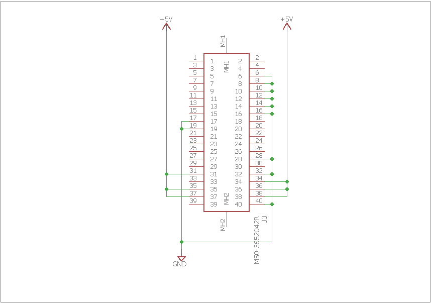
This wasn’t very helpful. All the remaining pins connected to either the FPGA or both the FPGA and the PIC. Then I noticed where on the PIC those pins were connected:
PIC pins connected to the machine control panel’s 40-pin connector.
Turns out that the PIC16C67 has a parallel target-mode interface that makes it look like a memory or other simple peripheral device to an external CPU and these pins were connected to the 40-pin connector.
It wasn’t a given this was used on the machine control panel, but I thought it was the most obvious and therefore the most likely solution and worth a try. I revised my pinout accordingly to show the location of the read, write, and and data pins. I also gave the remaining FPGA pins unique names:
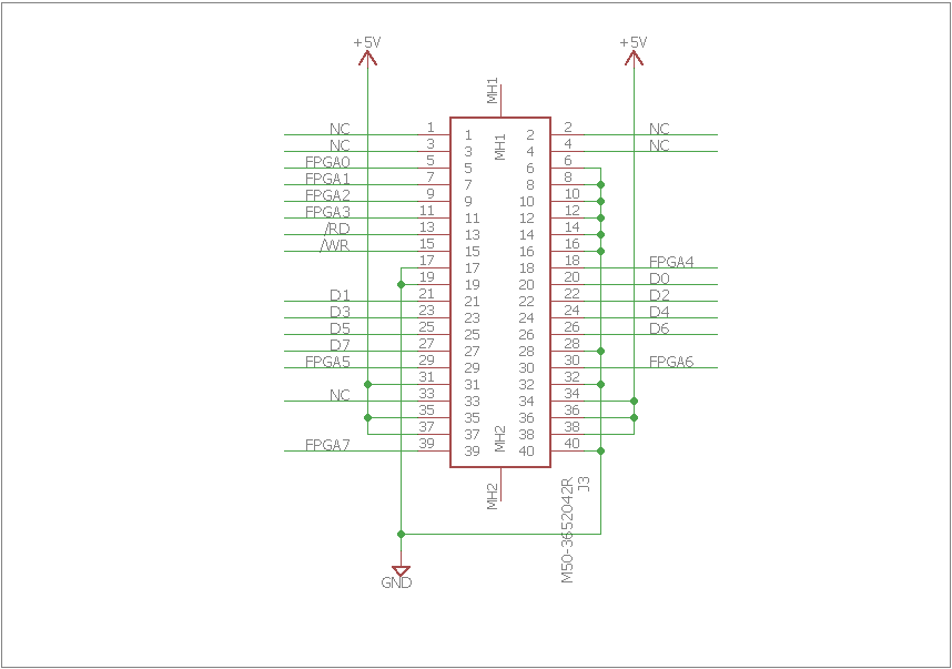
The most likely machine control panel pinout.
Crosspoint Switch Matrix Panel Interface Connector
I then turned my attention to the 40-pin connectors on the crosspoint switch matrix board. Were these the same pinout? Could I use the same hardware to talk to both the machine control panel and the crosspoint switch matrix panel?
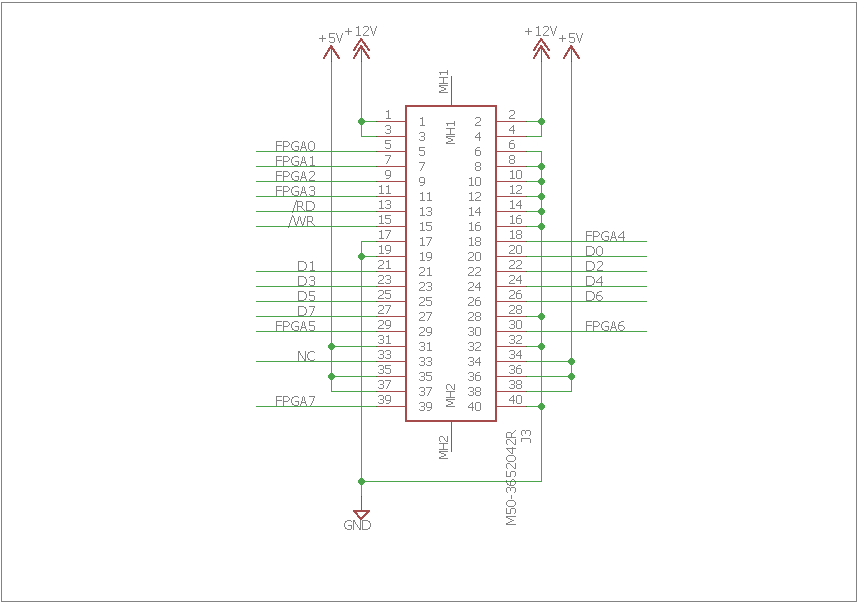
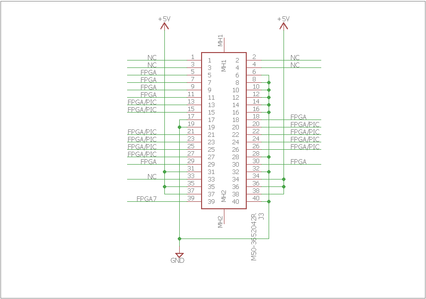
The crosspoint switch matrix panel’s 40 pin connector has the same pin out as the machine control panel with the exception of four 12 volt power pins.
After studying the 40-pin connectors on the crosspoint switch matrix panel, I determined that they used the same pin out as the machine control panel except that four of the no connects on the machine control panel connector were +12 volt power pins on the crosspoint switch matrix panel.
Another determination I made at this point is that the single board computer connected to the right connector on the panel and downstream panels connected to the left connector on the panel. I only learned this because there was a buffer on the data lines that, while it could be enabled and disabled, it was unidirectional and could only buffer data from the right connector to the left connector.
Putting it All Together
After finalizing the pin outs of the 40-pin connectors, I figured the 8 FPGA pins were likely chip selects or address pins and there were few enough of them that it made sense to build a board to try to talk to the machine control panel and crosspoint switch matrix panel from my own hardware.
Building an Interface Board
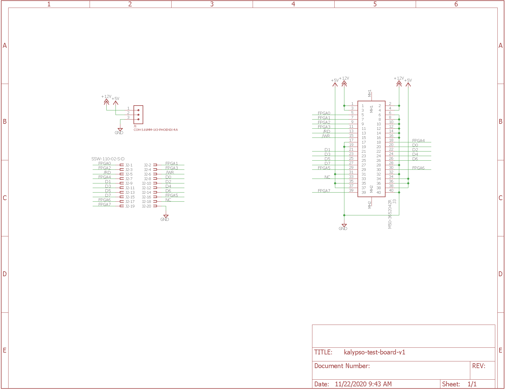
Breakout board schematic.
There’s not much to the board. The board breaks out the power pins on the 40-pin, 1.27 mm pitch connector to pins on a 3 position, 3.81 mm pitch Phoenix screw terminal strip header and the data pins to a 20-pin, 0.1″ pitch header.
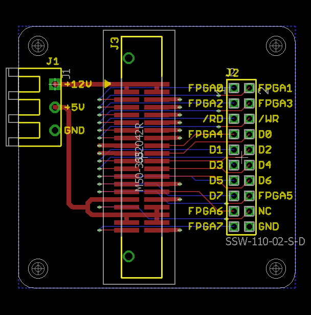
Breakout board layout.
The completed breakout board:
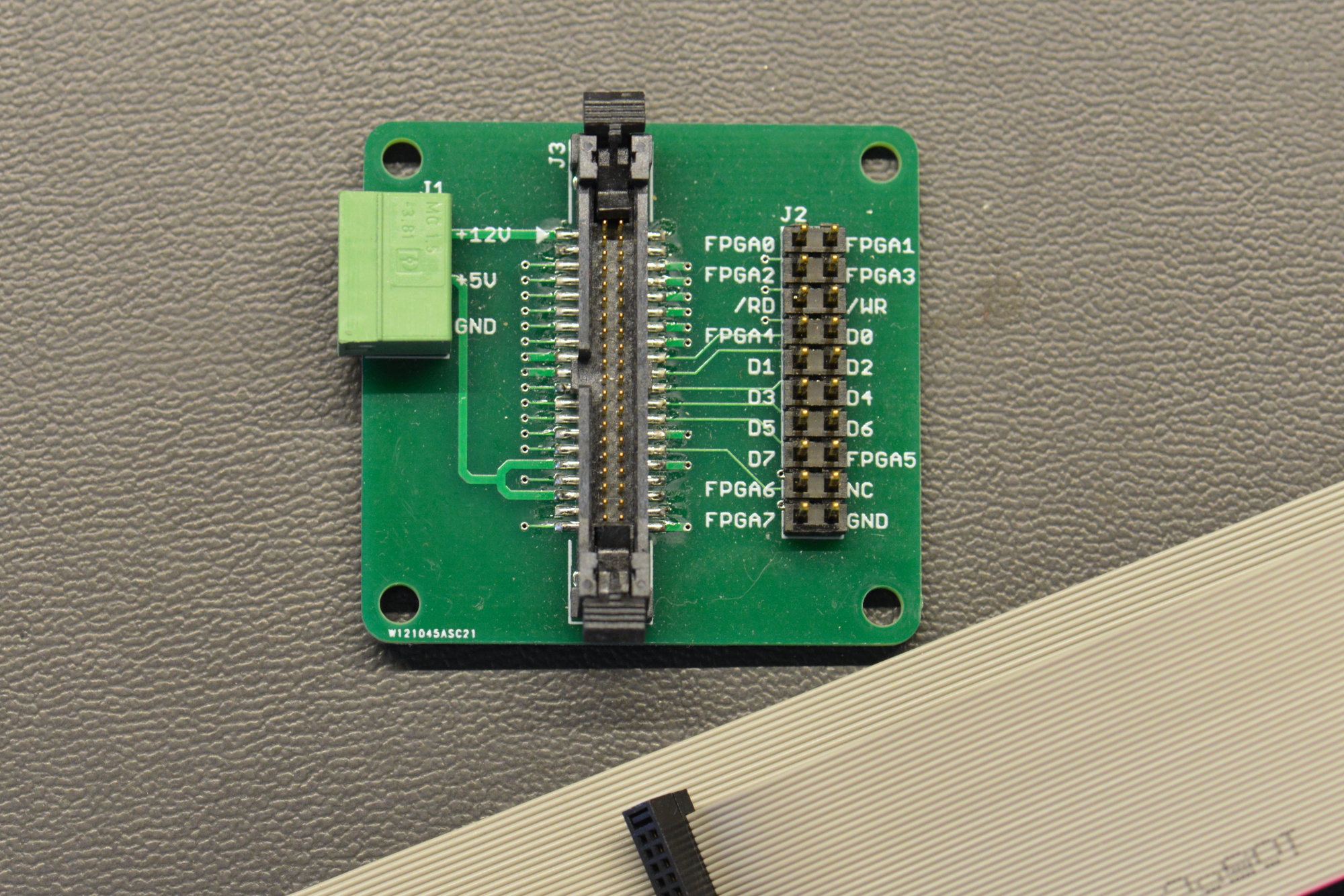
The completed breakout board.
Reverse Engineering the Machine Control Panel Protocol

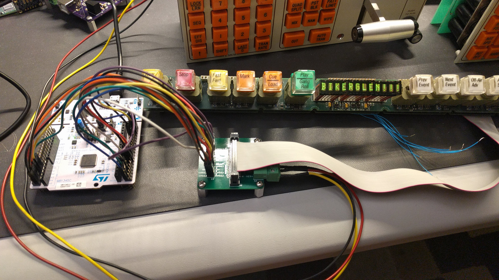
The test setup for probing the machine control panel’s forty pin connector.
With the breakout board complete, it was time to try to talk to the PIC on the machine control panel. I hooked up the breakout board to the machine control panel using a 40-pin ribbon cable and to a ST Microelectronics STM8 Nucleo 64 eval board using some jumper wires.
I also soldered some wires to the read, write, and chip select lines on the PIC’s secondary 40-pin footprint so that I could determine when the chip select line was asserted with an oscilloscope. Not shown in the photo above is the connection between the breakout board and my bench power supply that was used to supply +5 volts for the machine control board’s power.
Finding the PIC Chip Select
I wrote some software to search through various combinations of asserting and de-asserting the 8 FPGA pins while looking for the PIC’s chip select line to be asserted low. The PIC’s chip select was asserted low when the FPGA[7:0] pins were ‘b1000xxx0. Based on some more probing, I determined FPGA[0] was the active-low chip select for the board and the remaining pins except FPGA[7] were likely address pins.
Fault Light
While searching for the PIC’s chip select, I discovered that bringing FPGA7 low then high again after a few milliseconds caused the fault light on the machine control panel to turn off. I decided FPGA7 was an active low reset for the machine control panel. My pinout for the 40-pin connector now looked like this:
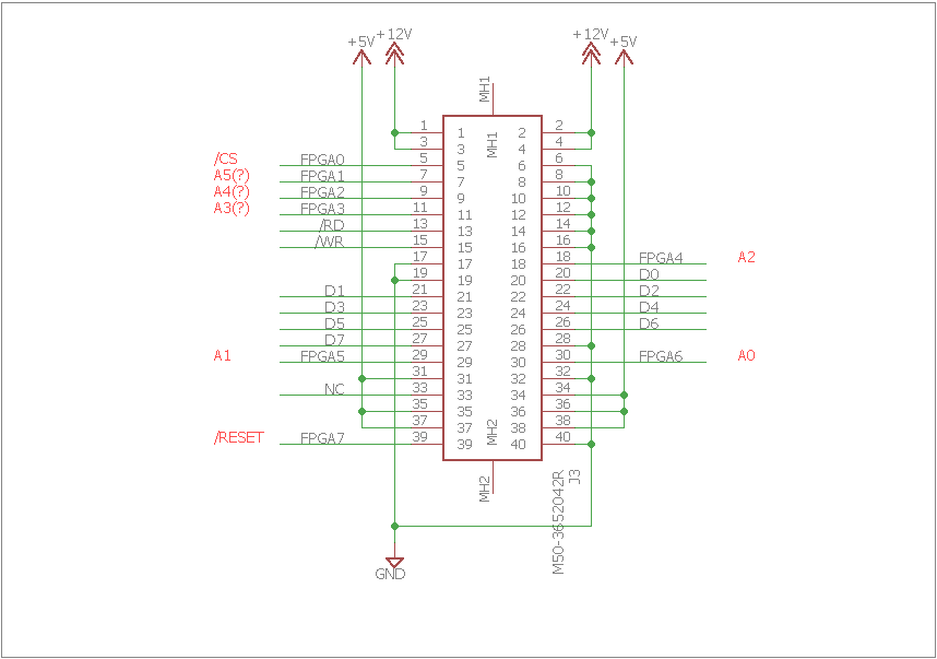
Updated 40-pin connector pin out based on early experiments.
I then modified my code to toggle the reset line to turn off the fault light then to write varying pseudorandom byte sequences to the PIC to try to turn on the tally lights or write text to the display. Nada, zilch, nothing.
Buttons
If I couldn’t write anything to the PIC, I decided I’d try to read something from the PIC. I changed my STM8 software to read bytes from the PIC then print them out the STM8’s serial port for display in a terminal window. I kept getting the same nine-byte pattern over and over again:
80 06 9F 00 00 80 00 FE A3
If I pushed a key, I’d get a different response then back to the same old pattern:
80 0F 91 0E 0F CF FF FF FF FF FF 9F 00 00 80 00 FE 24
Then when I released the key:
80 0F 91 0F 0F CF FF FF FF FF FF 9F 00 00 80 00 FE 25
Then when I pushed a different key:
80 0F 91 0F 0B CF FF FF FF FF FF 9F 00 00 80 00 FE 21
And released the key:
80 0F 91 0F 0F CF FF FF FF FF FF 9F 00 00 80 00 FE 25
Those look like packets! I decided the packet format looked like the following:
| Byte | Name | Notes |
|---|---|---|
| 0 | Start of Packet | 0x80 |
| 1 | Length | Excludes SOP, Length, and Checksum |
| 2 | Command Code | |
| 3 … Length+1 | Data Bytes | |
| Length+2 | Checksum | Modulo 256 sum of all bytes excluding the start of packet byte and the checksum byte. |
LED Display
With the initial packet format figured out, it was time to try writing packets in this same format to the PIC. I tried writing packets with varying lengths and command codes with all zero data, all 0xFF data, and all pseudorandom data. Still no dice and I was beginning to lose hope that I could talk to these panels.
As a last ditch effort, I fed the keypress packet back to the PIC but cycled through the command codes and first data byte. I let this run for a while then toward the end of the night I looked over and the LED display had some junk on it. I quickly narrowed down the packet that put the junk on the display then narrowed down the actual bytes required and wrote my own message to the display.
Success! The first meaningful message I wrote to the LED display.
The packet I sent to write this message was:
80 0f a1 00 42 49 4b 45 52 47 4c 45 4e 21 21 21 fe 24
Turns out, there’s an end of packet character too. The 0xFE is the end of packet character and must be there for the PIC to respond to any packets. I revised the packet format:
| Byte | Name | Notes |
|---|---|---|
| 0 | Start of Packet | 0x80 |
| 1 | Length | Excludes SOP, Length, and Checksum |
| 2 | Command Code | |
| 3 … Length | Data Bytes | |
| Length+1 | End of Packet | 0xFE |
| Length+2 | Checksum | Modulo 256 sum of all bytes excluding the start of packet byte and the checksum byte. |
Tally Lights

Slowly getting the tally lights to work.
I then repeated the process with my new found knowledge and eventually got a tally light to turn on:
80 05 a6 00 0d ff fe 35
And off:
80 05 a6 00 0d 00 fe 35
The command code is 0xA6. The 0x0D is the tally light number to turn on or off. The byte after the tally light number turns the tally light on (0xff) or off (0x00). I tried these same tally light packets on the crosspoint switch matrix panel and they worked there as well.
I also learned that none of the tally lights would work until the following packet was sent to the PIC. I don’t know exactly what it does:
80 02 a4 fe a4
I eventually learned that there’s one more nuance to the packet format. The final packet format incorporates a command length byte after the command code byte as one of the data bytes. This is 0x0C for the LED display command code and 0x02 for the tally light command code. For example:
80 0f a1 0c 42 49 4b 45 52 47 4c 45 4e 21 21 21 fe 30
And:
80 05 a6 02 0d ff fe 37
Reverse Engineering the LCD Backlight Hardware and Protocol
After achieving success with the alphanumeric LED display and tally lights on both panels, I turned my attention to the LED backlights for the LCD display on the crosspoint switch matrix panel.

A partial schematic of the logic on the back of the LCD module.
The first step was to create a partial schematic of the logic on the rear of the LCD focused on how the clock, latch, and data pins on the Allegro Microsystems A6275ELW 8-channel constant-current LED drivers connected to the reset of the system. I came up with the above partial schematic.
Unlike the alphanumeric displays on the machine control panel and the tally lights on both panels, the backlight driver serial data inputs and LCD data pins were connected directly to the data pins on the 40-pin connector bypassing the PIC microcontroller altogether. The chip selects, however, were a bit of convoluted mess involving both the Altera PLD and the logic gates on the LCD board.
Writing address 0x06 latched the lower two bits of the data bus into what I’m calling the LCD_SELECT register. This register is used to select one of three LCD controllers to write or to write to the backlight drivers.
| LCD_SELECT | Addressed Device |
|---|---|
| ‘b00 | LCD controller 0 (Windows 0 to 2 on display.) |
| ‘b01 | LCD controller 1 (Windows 3 to 5 on display.) |
| ‘b10 | LCD controller 2 (Windows 6 and 7 on display.) |
| ‘b11 | LCD reset and LED backlight clock/latch/data |
After discovering the LCD_SELECT register, I discovered two more valid addresses in the address map at addresses 0x04 and 0x05. I figured these were the LCD command and data registers. Since most LCD controllers have their command/data select signal low for command and high for data, I labeled address 0x04 LCD_CMD and address 0x05 LCD_DATA.
My guess at this point was that setting LCD_SELECT to ‘b00 and writing a byte to the LCD_CMD or LCD_DATA addresses would write a command or data byte into the first LCD controller. Likewise for an LCD_SELECT of ‘b01 and the second controller and an LCD_SELECT of ‘b10 and the third LCD controller.
With LCD_SELECT set to ‘b11, however, writing to either the LCD_CMD or LCD_DATA addresses caused the enable input of IC1B in the schematic above to be asserted. Then, depending on bits 7 and 6 of the write data, one of its Y0, Y1, Y2, or Y3 outputs would be asserted.
Y0 was attached to the LCD controllers’ reset pins. Y1 was attached to the A6275s’ clock input. Y2 was attached to the A6275s’ latch input. Y3 was not connected. Each of the four lowest data bus bits was connected to the serial data input on one of the four A6275 LED drivers.

The backlight is very flexible. Each LCD window is split into a top half and a bottom half and can be set to red, green, or amber separately.
I came up with the following algorithm to set the backlights:
- Write 0x03 to LCD_SELECT.
- To shift four bits of data into the four A6275s in parallel:
- Set bit 6 of a byte to ‘1’.
- Set bits 3:0 of the byte to the values to shift into the four A6275’s in parallel.
- Write this byte to LCD_DATA
- Repeat step 2 above a total of 8 times to shift a total of 32 bits into the four A6275’s.
- Write 0x80 to LCD_DATA to transfer the shifted data from the A6275’s shift registers into the A6275’s output latches and drivers.
Then it was just a matter of mapping the bits being shifted out to which backlight LED’s they controlled and writing a function to set the backlights:
void SetLcdBacklights (uint8_t side, uint8_t display, uint8_t redtop, uint8_t redbot, uint8_t grntop, uint8_t grnbot)
{
    int i;
    uint8_t d;

    // set up for FPGA writes
    WriteFpgaBegin ();

    WriteFpga (side, LCD_SELECT, display | 0x03); // select display number and backlights

    // clock out data serially
    for (i = 0; i < 8; i++) {
        d = 0;
        d |= (redtop & 0x80) ? 8 : 0;
        d |= (redbot & 0x80) ? 4 : 0;
        d |= (grntop & 0x80) ? 2 : 0;
        d |= (grnbot & 0x80) ? 1 : 0;
        WriteFpga (side, LCD_DATA, 0x40 | d);
        redtop <<= 1;
        redbot <<= 1;
        grntop <<= 1;
        grnbot <<= 1;
    }

    // create high pulse on A6275 latch
    WriteFpga (side, LCD_DATA, 0x80);
}
This worked and I had control of the LED segments used for the LCD backlight!
Reverse Engineering the LCD Display Protocol
At this point, I can:
- Read button presses on both panels
- Control the tally lights on both panels
- Write to the machine control panel’s alphanumeric LED display
- Control the LCD backlight on the crosspoint switch matrix panel
In short, I can control everything except for that glorious, bespoke eight-window LCD display. I can even write to the LCD command and data registers on each of the three controllers but this is useless without knowing the display initialization commands. And I can’t figure out the display initialization commands without knowing what LCD controller IC is under each of three blobs on the LCD display board. Or can I?
Finding Similar, Working Hardware
Time to go back to eBay. I needed to find a 4-M/E Kalypso console with a working controller board. With a working Kalypso console, I could probe the 40-pin connection between the single board computer and the crosspoint switch matrix panel with a logic analyzer and snag the LCD initialization codes.
My Grass Valley Kalypso 1-M/E control surface.
I found several complete Kalypso 4-M/E consoles for sale but they were expensive, shipping was by freight, and I don’t have room for one in my house. I decided the next best thing would be the smaller single mix-effects version, the Kalypso 1-M/E. The 1-M/E console is usually used alongside the larger 2-M/E and 4-M/E consoles.
For example, the technical director can delegate one of the mix-effects boards in the k-frame to the operator of this console. This is useful for complicated live productions where a single person may not be able to set up all the effects. It’s also useful to allow a second, smaller studio to re-use some of the k-frame hardware when the main studio is not in use.
I ordered it and it arrive. I got a flashlight and peaked inside the ventilation slots. No dice. Entirely different architecture. Instead of a 40-pin, 1.27 mm pitch connector, the 1-M/E used what looked like a 60-pin, 0.1″ pitch connector between the CPU board and the board with all the knobs and buttons and lights. At some point I’ll do a teardown of the 1-M/E.
My Kalypso local aux panel.
I went back to eBay. I found a working Local Aux Panel for sale. The local aux panel can be used to switch the video sources for miscellaneous displays in the studio. One use is to switch the video shown on the teleprompters or other displays on the studio floor.
The local aux panel guts. Note the 40-pin connector at the left.
I ordered it, it arrived, and I took it apart. Sure enough, it has a 40-pin connector! I used a DMM’s continuity test function to verify the powers and grounds were in the same spots as on the crosspoint switch matrix and machine control panel. They were!
Logic Analyzer Breakout Board
The next step was to build another breakout board that would allow me to probe the 16 or so pins of interest between the CPU board and the user input output board with a logic analyzer. The schematic is just three connectors and connecting matching pin numbers together between the three connectors:
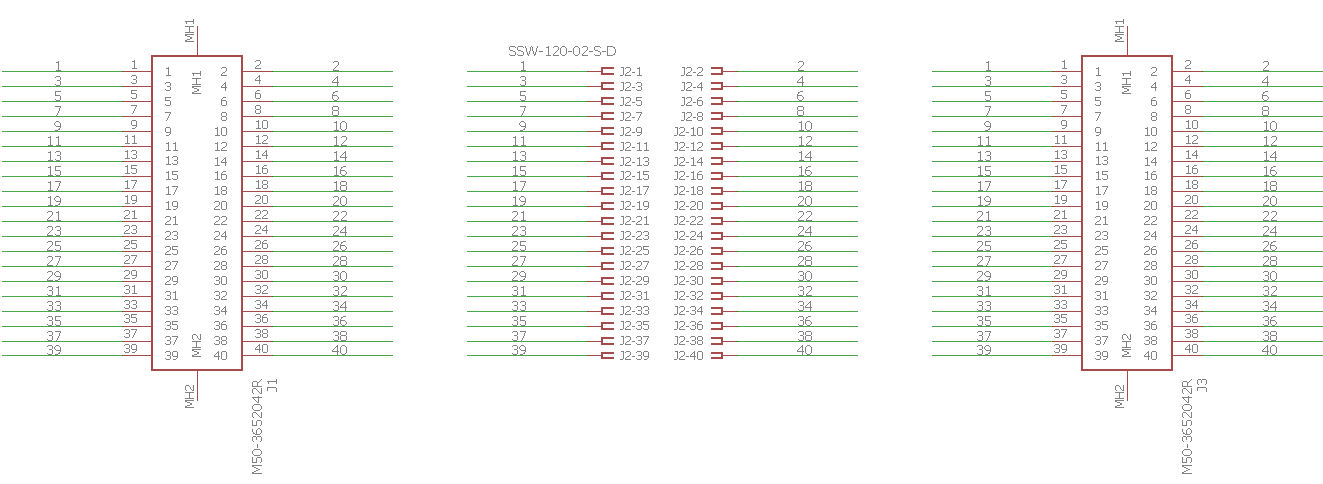
Logic analyzer breakout board schematic.
The board layout:
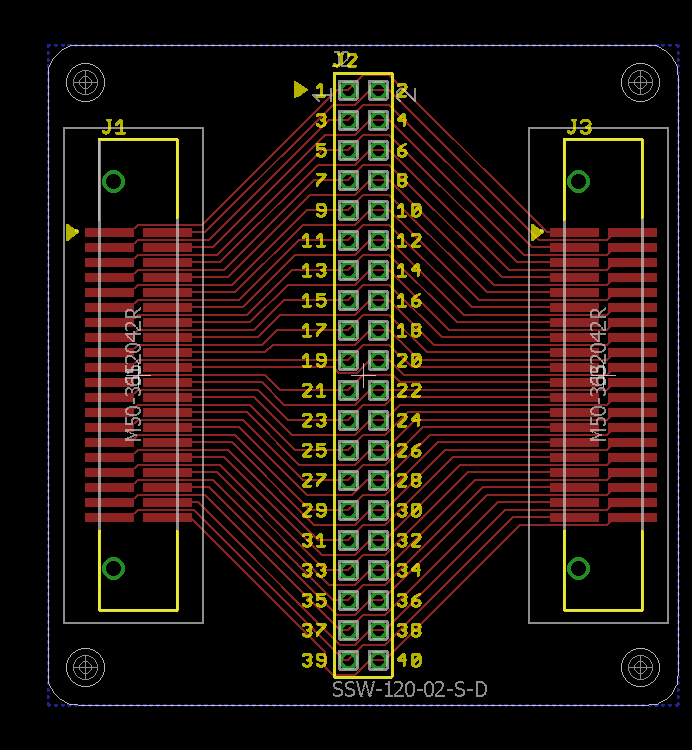
Logic analyzer breakout board board layout.
And the finished board:
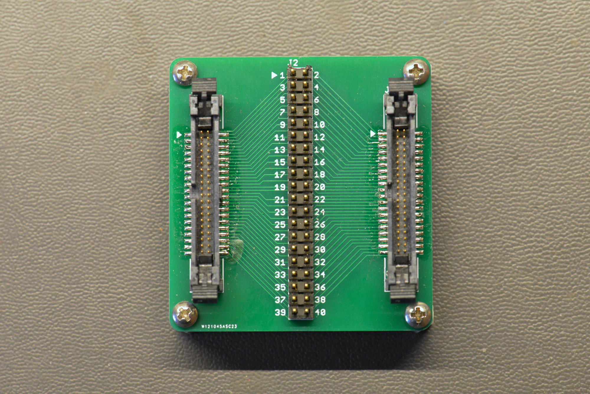
Logic analyzer breakout board.
Capturing the Display Initialization Commands with the Logic Analyzer
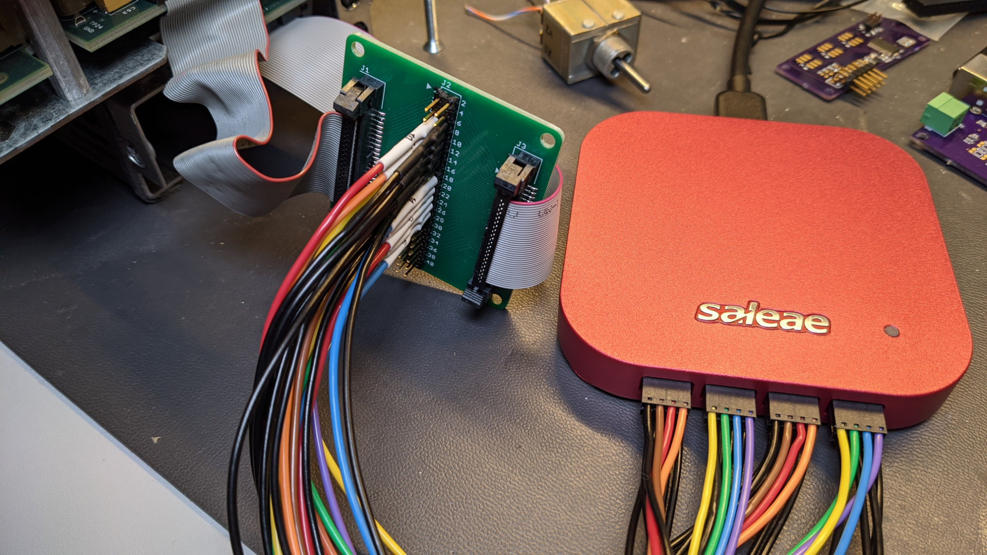
Using the Saleae Logic 16 Pro to capture the display initialization commands.
I hooked the breakout board up between the local aux panel’s CPU board and user input output board and connected my Saleae Logic 16 Pro to the breakout board. I started the logic analyzer capture then powered up the local aux panel. On the first, run I captured the magical incantation to initialize each of the three display controllers on each LCD display module.
Display Controller 0:
0xAE 0x40 0xA1 0xA6 0xA4 0xA3 0xC8 0x2D 0xAC 0xAF
Display Controller 1:
0xAE 0x40 0xA1 0xA6 0xA4 0xA2 0x28 0xAC 0xAF
Display Controller 2:
0xAE 0x40 0xA1 0xA6 0xA4 0xA2 0x28 0xAC 0xAF
These initialization commands are very similar to the commands used by the Sitronix ST7565P LCD controller but there’s an extra command code in there that is not documented in the Sitronix ST7565P datasheet so it’s likely not the Sitronix part. The Sitronix part is likely a decade newer too.
I wrote a C function to initialize each of the three display controllers on the LCD module:
void InitLcd (uint8_t side, uint8_t display)
{
    // set up for FPGA writes
    WriteFpgaBegin ();

    // select display and controller 0
    WriteFpga (side, LCD_SELECT, display | 0x00);

    // write command registers
    WriteFpga (side, LCD_CMD, 0xAE);         // display off
    WriteFpga (side, LCD_CMD, 0x40);         // page address
    WriteFpga (side, LCD_CMD, 0xA1);         // scan direction = reversed
    WriteFpga (side, LCD_CMD, 0xA6);         // inverse display = normal
    WriteFpga (side, LCD_CMD, 0xA4);         // all pixel on = normal
    WriteFpga (side, LCD_CMD, 0xA3);         // bias = 1/7
    WriteFpga (side, LCD_CMD, 0xC8);         // com direction = reversed
    WriteFpga (side, LCD_CMD, 0x2D);         // power control = VB, VF
    WriteFpga (side, LCD_CMD, 0xAC);
    WriteFpga (side, LCD_CMD, 0xAF);         // display on

    // select display and controller 1
    WriteFpga (side, LCD_SELECT, display | 0x01);

    // write command registers
    WriteFpga (side, LCD_CMD, 0xAE);
    WriteFpga (side, LCD_CMD, 0x40);
    WriteFpga (side, LCD_CMD, 0xA1);
    WriteFpga (side, LCD_CMD, 0xA6);
    WriteFpga (side, LCD_CMD, 0xA4);
    WriteFpga (side, LCD_CMD, 0xA2);
    WriteFpga (side, LCD_CMD, 0x28);
    WriteFpga (side, LCD_CMD, 0xAC);
    WriteFpga (side, LCD_CMD, 0xAF);

    // select display and controller 2
    WriteFpga (side, LCD_SELECT, display | 0x02);

    // write command registers
    WriteFpga (side, LCD_CMD, 0xAE);
    WriteFpga (side, LCD_CMD, 0x40);
    WriteFpga (side, LCD_CMD, 0xA1);
    WriteFpga (side, LCD_CMD, 0xA6);
    WriteFpga (side, LCD_CMD, 0xA4);
    WriteFpga (side, LCD_CMD, 0xA2);
    WriteFpga (side, LCD_CMD, 0x28);
    WriteFpga (side, LCD_CMD, 0xAC);
    WriteFpga (side, LCD_CMD, 0xAF);
}
Next I needed to know where in display memory each of the 8 windows on the LCD were located. I did another capture and came up with the following table:
SI_SEGMENT_VARIABLE(lcd_cmds[8][13], const uint8_t, SI_SEG_CODE) = {
 { 0, 0xb0, 0x11, 0x00, 0xb1, 0x11, 0x00, 0xb2, 0x11, 0x00, 0xb3, 0x11, 0x00 },
 { 0, 0xb0, 0x13, 0x00, 0xb1, 0x13, 0x00, 0xb2, 0x13, 0x00, 0xb3, 0x13, 0x00 },
 { 0, 0xb0, 0x15, 0x00, 0xb1, 0x15, 0x00, 0xb2, 0x15, 0x00, 0xb3, 0x15, 0x00 },
 { 1, 0xb0, 0x10, 0x05, 0xb1, 0x10, 0x05, 0xb2, 0x10, 0x05, 0xb3, 0x10, 0x05 },
 { 1, 0xb0, 0x12, 0x05, 0xb1, 0x12, 0x05, 0xb2, 0x12, 0x05, 0xb3, 0x12, 0x05 },
 { 1, 0xb0, 0x14, 0x05, 0xb1, 0x14, 0x05, 0xb2, 0x14, 0x05, 0xb3, 0x14, 0x05 },
 { 2, 0xb0, 0x10, 0x05, 0xb1, 0x10, 0x05, 0xb2, 0x10, 0x05, 0xb3, 0x10, 0x05 },
 { 2, 0xb0, 0x12, 0x05, 0xb1, 0x12, 0x05, 0xb2, 0x12, 0x05, 0xb3, 0x12, 0x05 }
};
The index into the table is the LCD window number from 0 to 7. Byte 0 is the LCD controller number that controls the pixels on that window. Bytes 1 to 3 are the command code and two address data bytes that address the first 8 rows of pixels on the window. Bytes 4-6 address the second 8 rows of pixels. Bytes 7-9 address the third 8 rows of pixels. Bytes 10-12 address the last 8 rows of pixels.
With that information captured, it was time to write to the display. I wrote some test graphics but it just didn’t look quite right. The contrast was off and there was an odd vertical scrolling effect on the display.
Capturing the PIC Initialization Commands with the Logic Analyzer
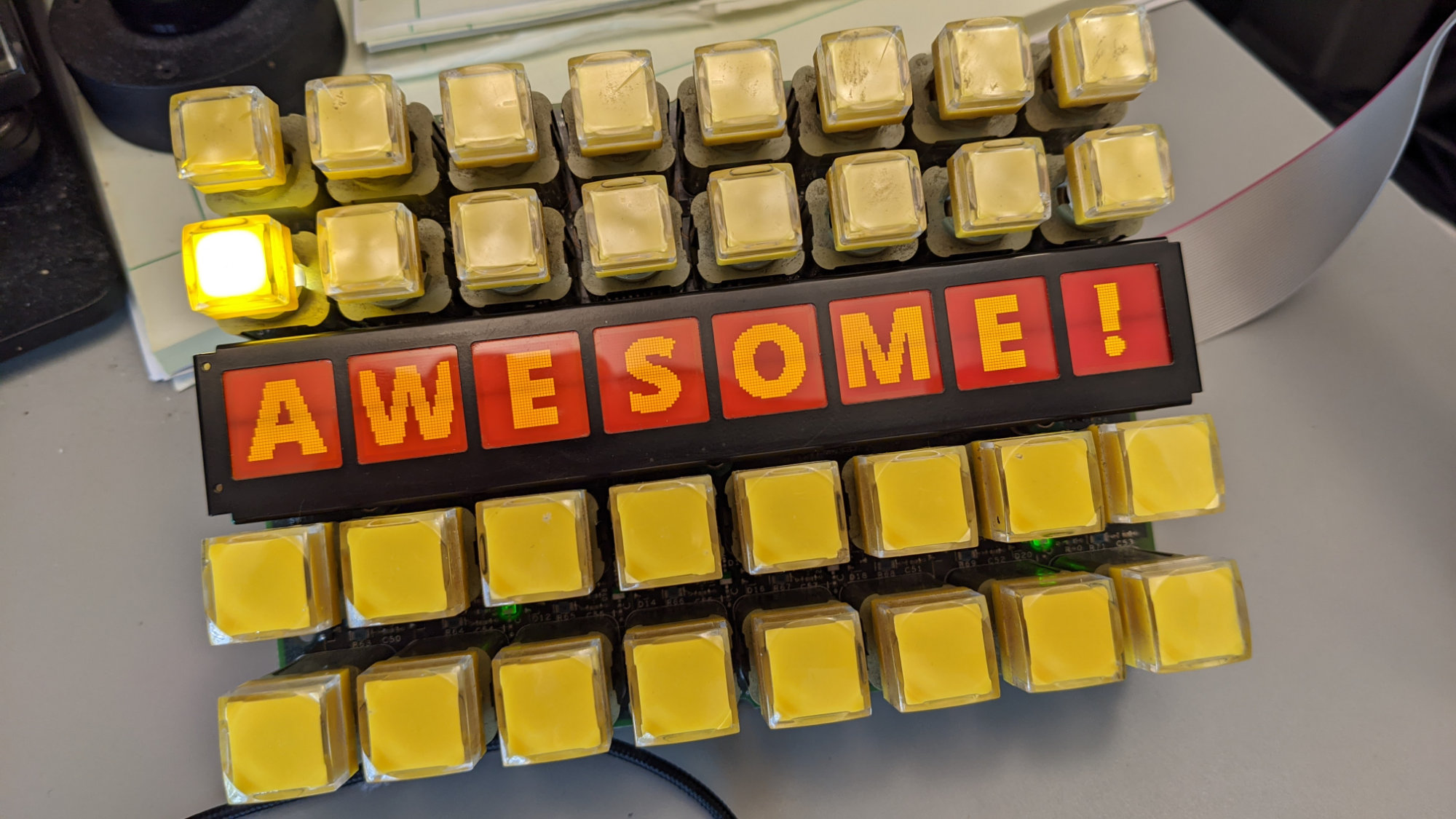
With everything configured properly, the display looks great!
My guess is that the PIC controlled the LCD contrast and something wasn’t quite configured right on the PIC. I decided to use the logic analyzer to capture a bit more data to see how the four PICs on the local aux panel were being initialized. I came up with the following packets that needed to be sent to the crosspoint switch matrix panel’s PIC and then the display looked, well, awesome!
// RESET (?)
SI_SEGMENT_VARIABLE(pic1_init_pkt_1[3], const uint8_t, SI_SEG_CODE) = {
    0x81, 0x00,
    0xFE
};

// UNKNOWN
SI_SEGMENT_VARIABLE(pic1_init_pkt_2[45], const uint8_t, SI_SEG_CODE) = {
    0xA7, 0x00,
    0xA5, 0x00,
    0xA4, 0x02, 0x02, 0xA2,
    0xA4, 0x02, 0x42, 0xA2,
    0xA4, 0x02, 0x02, 0xA2,
    0xA4, 0x02, 0x42, 0xA2,
    0xA4, 0x02, 0x02, 0xA2,
    0xA4, 0x02, 0x42, 0xA2,
    0xA4, 0x02, 0x02, 0xA2,
    0xA4, 0x02, 0x42, 0xA2,
    0xA4, 0x02, 0x02, 0xA2,
    0xA4, 0x02, 0x42, 0xA2,
    0xFE
};

// UNKNOWN
SI_SEGMENT_VARIABLE(pic1_init_pkt_3[33], const uint8_t, SI_SEG_CODE) = {
    0xA4, 0x02, 0x02, 0xA2,
    0xA4, 0x02, 0x42, 0xA2,
    0xA4, 0x02, 0x02, 0xA2,
    0xA4, 0x02, 0x42, 0xA2,
    0xA4, 0x02, 0x02, 0xA2,
    0xA4, 0x02, 0x42, 0xA2,
    0xA4, 0x02, 0x02, 0xA2,
    0xA4, 0x02, 0x42, 0xA2,
    0xFE
};

// SOMETHING + ENABLE TALLY LIGHTS + SET CONTRAST TO 27
SI_SEGMENT_VARIABLE(pic1_init_pkt_4[14], const uint8_t, SI_SEG_CODE) = {
    0xE5, 0x03, 0x13, 0x50, 0x01,
    0xA4, 0x02, 0x83, 0x21,
    0xA4, 0x02, 0xC3, 0x21,
    0xFE
};
Designing a USB Controller Board
Schematic
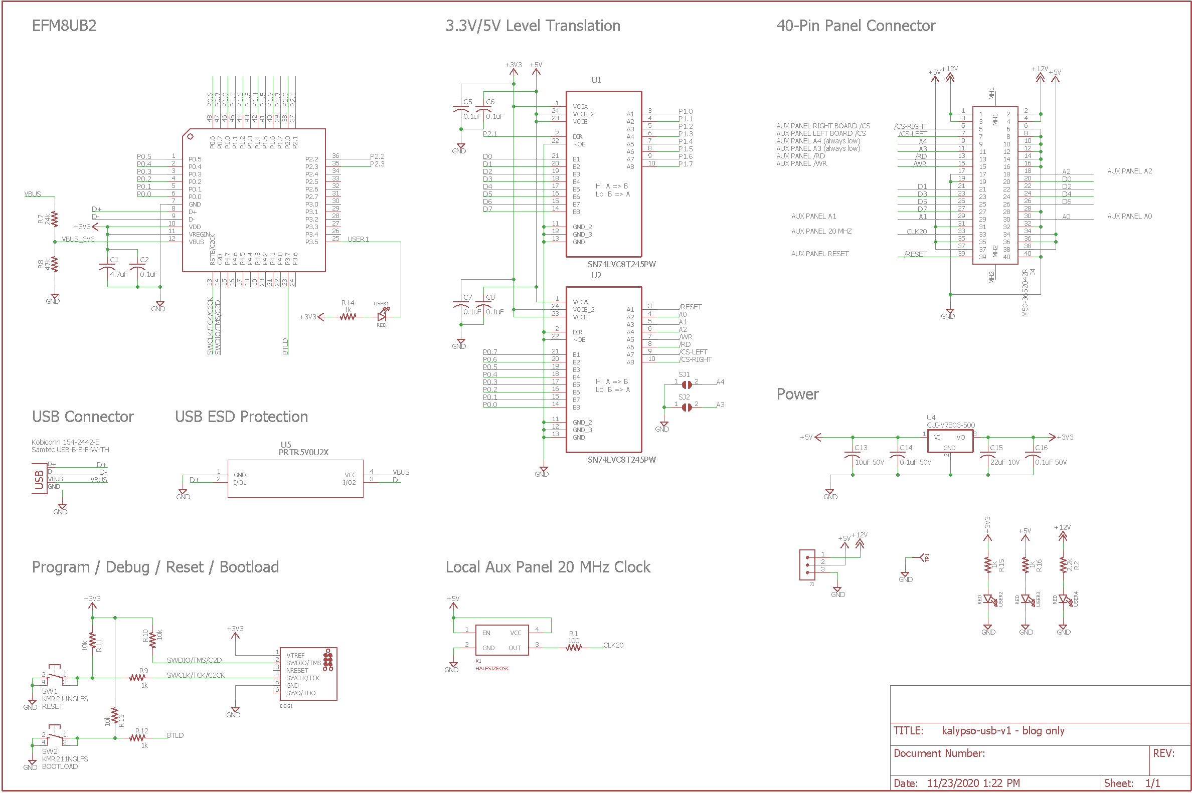
Schematic of my USB controller for the vintage Grass Valley hardware.
Microcontroller Selection
In the past I’ve used both the Microchip PIC16F1459 and the Silicon Labs EFM8UB1 for designs where I’ve needed USB connectivity. For this design, I’m going to use the Silicon Labs EFM8UB2 because I need more I/O pins than the other two devices have. Also, this project uses a graphic LCD module so the 64kB flash on the EFM8UB2 will be handy for storing fonts and canned images vs the 14kB flash on the PIC and the 16kB flash on the EFM8UB1.
Common Items
This design has all the items common to my other USB designs, namely a USB connector, ESD protection for the USB port, and a program / debug connector. For this design, I used a USB Type B receptacle. They’re cheap and rugged even if not as cool as USB Type C. For a programming connector, I’m using a Tag-Connect footprint again.
Interfacing to the Grass Valley Hardware
My hardware interfaces to the Grass Valley hardware is through J4 which is a 40-pin, 1.27 mm pitch connector. This connector connects to a ribbon cable that is used to connect to an identical 40-pin connector on either the machine control panel or the crosspoint switch matrix panel.
The EFM8UB2 is a microcontroller with 5 volt tolerant 3.3 volt I/O. The Grass Valley panels are all 5 volt I/O devices. To prevent issues with driving 5 volt inputs from 3.3 volt outputs I’m using Texas Instruments 74LVC8T245 logic level translators.
The translator for the chip selects, address bus, read, write, and reset signals have their direction and output enable pins tied low so these signals are always routed from the EFM8UB2 to the 40 pin connector. The translator for the data bus has its output tied low so it is always enabled but its direction pin is connected to the EFM8UB2 allowing the EFM8UB2 to route data from the itself to the 40-pin connector for writes or from the 40-pin connector to itself for reads.
Note that level translator U1 is “flipped” relative to level translator U2 on the schematic because its DIR pin needs to be connected to the EFM8UB2 and the DIR pin is referenced to VCCA. This requires that the rest of the 3.3 volt “A” side of the part connects to the EFM8UB2 too.
After studying the local aux panel hardware some, I learned that I could control it using this same hardware if I supplied a second chip select (/CS-LEFT) and a 20 MHz clock (CLK20). I also determined that for all my hardware, I could tie A4 and A3 low and save two pins on the EFM8UB2 and avoid the need for a third logic level translator IC. I tied these two pins low through some solder jumpers to make it easier to connect them later if needed. They’re probably necessary if I ever try to daisy chain two crosspoint switch matrix panels together.
Power Supply
This project is a USB self-powered design rather than a USB bus-powered design. If a 5 volt and 12 volt power supply are connected to J1, this board can supply power over the ribbon cable to smaller panels like the machine control panel or a single crosspoint switch matrix panel. The board can be backpowered from larger panels like the local aux panel or a string of crosspoint panels powered through their 10 pin header connectors. I included LEDs to indicate that the three power supply voltages are present.
Board Layout
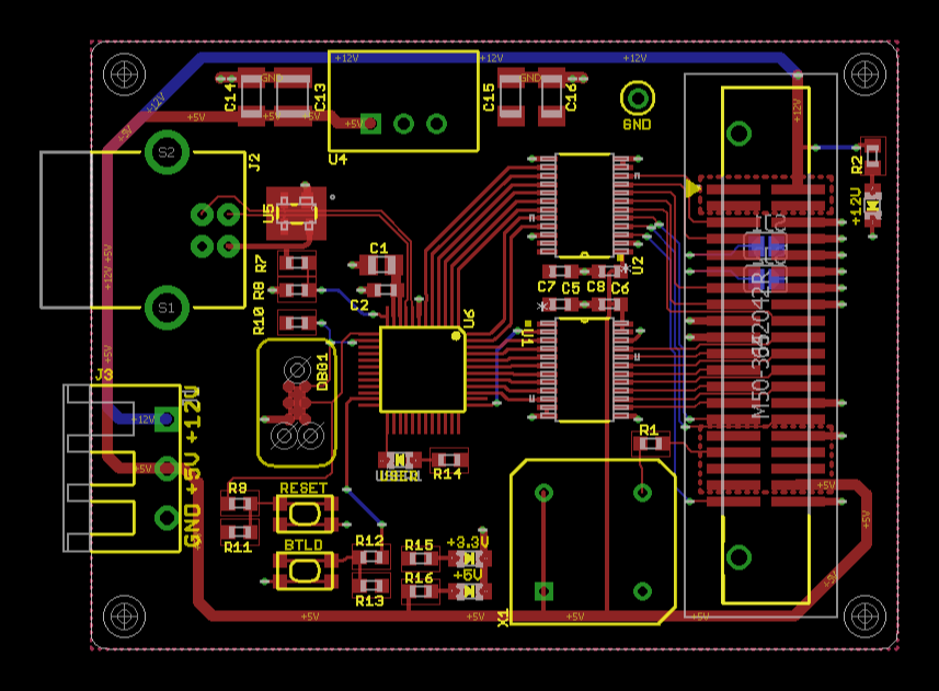
Finished board layout.
The board layout flows from left to right with power and USB inputs on the left and the connector to the machine control panel or crosspoint switch matrix panel on the right. Onc the layout was complete, I uploaded the boards to OSH Park to generate a preview.
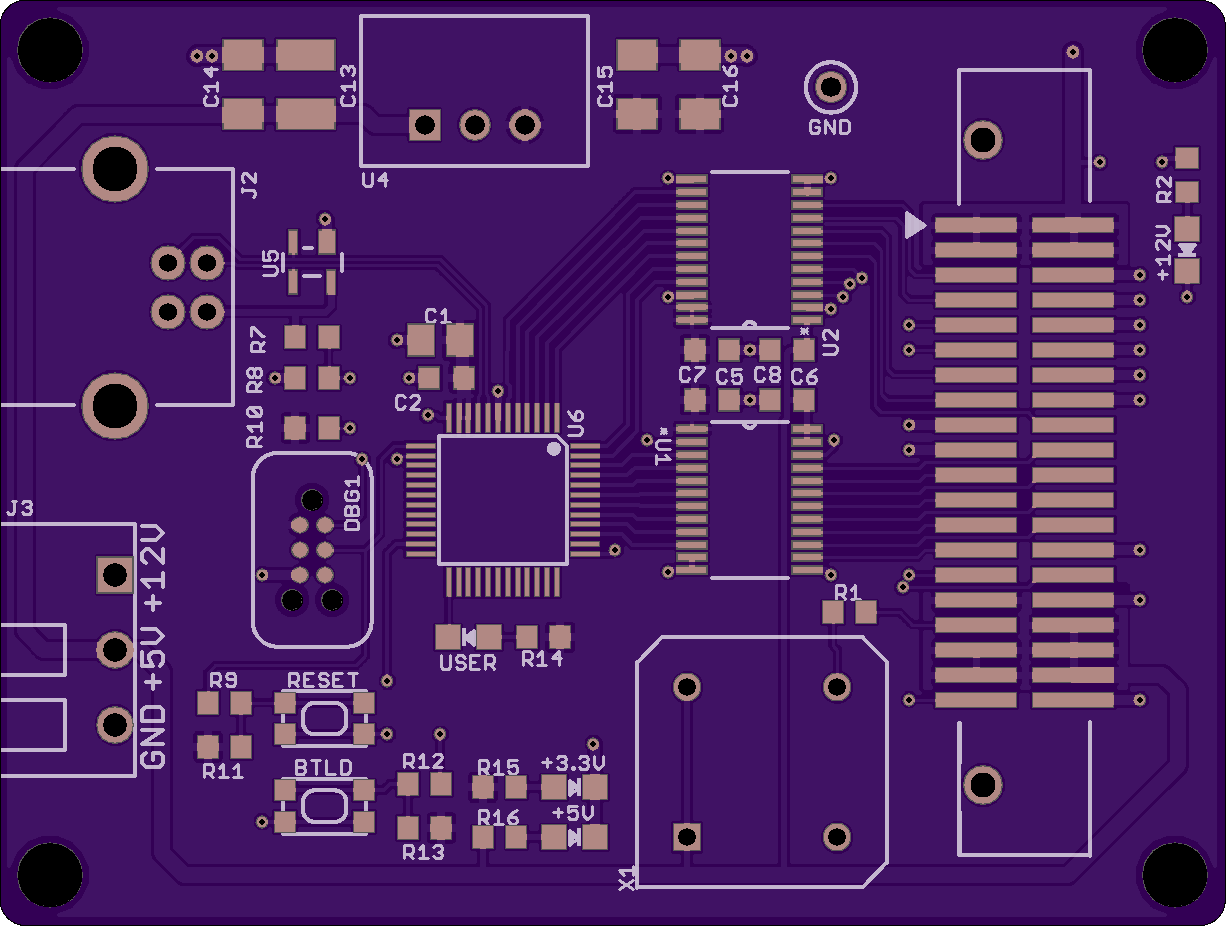
OSH Park preview of the top / component side of the board. A bit of an oops on the power connector silkscreen.
Above is preview of the top of the board.
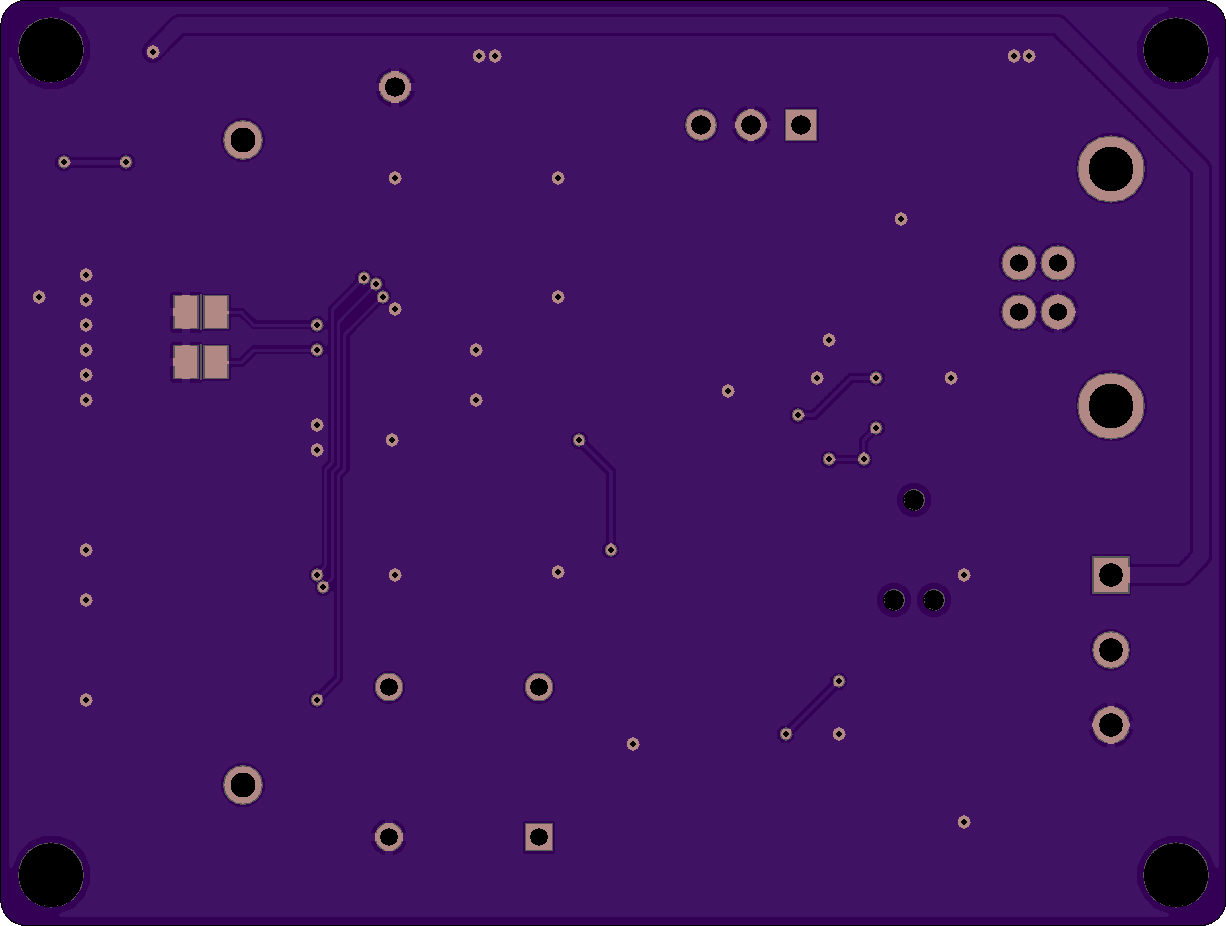
OSH Park preview of the bottom / solder side of the board.
Above is preview of the bottom of the board. Once I was happy with the previews, I ordered the boards.
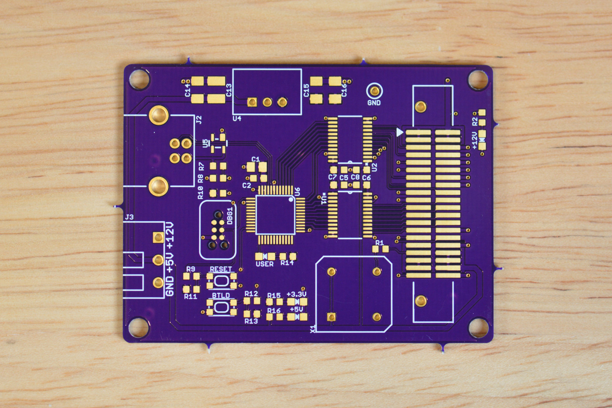
The blank board back from OSH Park.
As usual, the board from OSH Park looked great!
Assembly
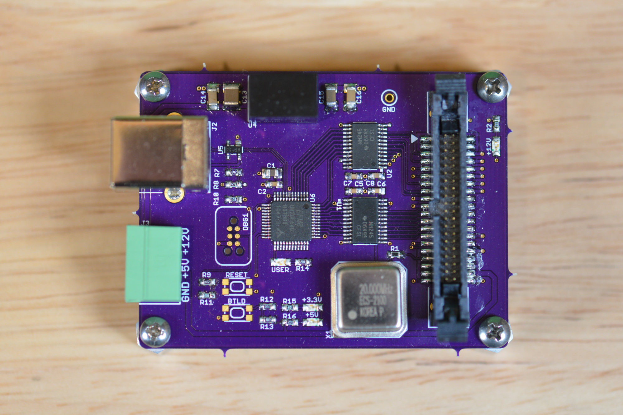
One of the stuffed boards.
I built up two of the boards; one with green LEDs and the second with yellow LEDs. I’m going to build up a third with red LEDs. Who needs serial numbers when I have more different colors of LEDs than I have boards. Anyway, time to work on the software!
The USB Controller Software
There are two version of software for the USB controller. One version is for use with the machine control panel and the other version is for use with the crosspoint switch matrix panel. Both function fairly similar and only differ in what types of USB reports they can process and how they control the capabilities of the underlying hardware.
The code is available on Github (see the end of this post). Rather than delving into the code in detail here, I’d like to focus on the USB reports that each version supports and how these USB reports monitor and control the underlying Grass Valley hardware.
Machine Control Panel USB Reports
The table below summarizes the USB IN and USB OUT reports used to monitor and control the machine control panel.
| Report ID | Report Direction | Report Length (Bytes) | Details |
|---|---|---|---|
| 1 | IN | 8 | Key Press Report |
| 2 | OUT | 12 | Set LED Display Text |
| 3 | OUT | 4 | Set Tally Lights |
Key Press IN Report (0x01)
This report is sent from the device to the host whenever a key is pressed or released. The table below maps bits in the report to keys. A clear bit corresponds to a pressed key. A set bit corresponds to a released key. When the user definable switch panel is not connected to the machine control panel, its keys will be registered as pressed constantly. This does not affect the sending of reports since reports are only sent when keys are changed.
| Report Byte | Report Bit | Key |
|---|---|---|
| 0 | 0 | Rew |
| 0 | 1 | Stop |
| 0 | 2 | Fast Fwd |
| 0 | 3 | Mark |
| 1 | 0 | Cue / Load |
| 1 | 1 | Play / Gang Roll |
| 1 | 2 | Prev Event |
| 1 | 3 | Next Event |
| 2 | 0 | Off-Air Adv |
| 2 | 1 | Auto Start |
| 2 | 2 | Set Deleg |
| 2 | 3 | PVW Pri |
| 3 | 0 | Still Store |
| 3 | 1 | M/E 1 |
| 3 | 2 | M/E 2 |
| 3 | 3 | M/E 3 |
| 4 | 0 | Pgm Pst |
| 4 | 1 | Alt PVW |
Set LED Display Text OUT Report (0x02)
This report is sent form the host to the device to set the text on the 12-digit alphanumeric LED display on the machine control panel. The SLG2016 character set is included below for reference.
| Byte | Function |
|---|---|
| 0-11 | Display text. Byte 0 is left-most character, byte 11 is right-most character. The most-significant bit of each byte of the message is ignored. |
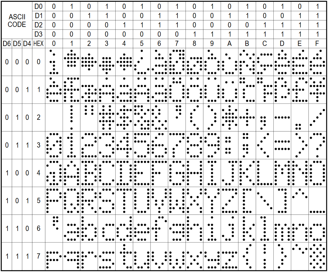
SLG2016 character map from the SLG2016 datasheet.
Set Tally Lights OUT Report (0x03)
This report is sent form the host to the device to set or clear the tally lights on the machine control panel. Set bits will illuminate their corresponding tally lights. Cleared bits will extinguish their corresponding tally lights.
| Report Byte | Report Bits | Function |
|---|---|---|
| 0 | 7:0 | Set or clear tally lights 31:24 |
| 1 | 7:0 | Set or clear tally lights 23:16 |
| 2 | 7:0 | Set or clear tally lights 15:8 |
| 3 | 7:0 | Set or clear tally lights 7:0 |
The machine control panel’s PIC microcontroller can set or clear up to 10 tally lights every 10 ms. The USB controller software keeps track of the state of the tally lights on the machine control panel and the commanded tally light states from these reports.
When differences are found between the commanded state and the actual state, the EFM8UB2 creates a packet to update up to 10 of the machine control panel’s tally lights at once. This process is repeated every 10 ms until the actual state matches the commanded state. For this reason, it can take up to 40 ms for all the tally lights to match their commanded state.
A mapping of machine control panel keys to tally lights is shown below.
| Report Byte | Report Bit | Tally Light Number | Tally Light Key |
|---|---|---|---|
| 2 | 2 | 10 | Rew |
| 2 | 3 | 11 | Stop |
| 2 | 4 | 12 | Fast Fwd |
| 2 | 5 | 13 | Mark |
| 2 | 6 | 14 | Cue / Load |
| 2 | 7 | 15 | Play / Gang Roll |
| 1 | 0 | 16 | Prev Event |
| 1 | 1 | 17 | Next Event |
| 1 | 2 | 18 | Off-Air Adv |
| 1 | 3 | 19 | Auto Start |
| 0 | 0 | 24 | Set Deleg |
| 0 | 1 | 25 | PVW Pri |
| 0 | 2 | 26 | Still Store |
| 0 | 7 | 31 | M/E 1 |
| 0 | 5 | 29 | M/E 2 |
| 0 | 3 | 27 | M/E 3 |
| 0 | 6 | 30 | Pgm Pst |
| 0 | 4 | 28 | Alt PVW |
Crosspoint Switch Matrix Panel USB Reports
The table below summarizes the USB IN and USB OUT reports used to monitor and control the crosspoint switch matrix panel.
| Report ID | Report Direction | Report Length (Bytes) | Details |
|---|---|---|---|
| 1 | IN | 8 | Key Press Report |
| 3 | OUT | 4 | Set Tally Lights |
| 4 | OUT | 4 | Set LCD Backlights |
| 5 | OUT | 21 | Set LCD Display Text |
| 6 | OUT | 33 | Set LCD Display Graphics |
Key and Tally Light Numbering
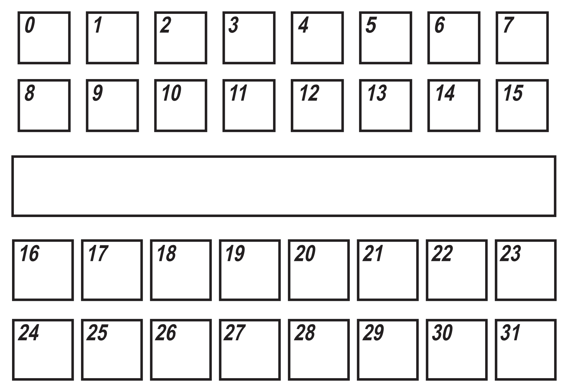
Crosspoint switch matrix panel key and tally light numbering.
Keys and tally lights are numbered as shown in the above diagram. This numbering scheme is used for both the key press and set tally lights reports below. It is also the numbering scheme used by the PIC16C67 microcontroller when sending packets to the PIC to turn tally lights on or off.
Key Press IN Report (0x01)
This report is sent from the device to the host whenever a key is pressed or released. The table below maps bits in the report to keys. A clear bit corresponds to a pressed key. A set bit corresponds to a released key.
| Report Byte | Report Bit | Key |
|---|---|---|
| 0 | 0 | 0 |
| 1 | 0 | 1 |
| 2 | 0 | 2 |
| 3 | 0 | 3 |
| 4 | 0 | 4 |
| 5 | 0 | 5 |
| 6 | 0 | 6 |
| 7 | 0 | 7 |
| 0 | 1 | 8 |
| 1 | 1 | 9 |
| 2 | 1 | 10 |
| 3 | 1 | 11 |
| 4 | 1 | 12 |
| 5 | 1 | 13 |
| 6 | 1 | 14 |
| 7 | 1 | 15 |
| 0 | 2 | 16 |
| 1 | 2 | 17 |
| 2 | 2 | 18 |
| 3 | 2 | 19 |
| 4 | 2 | 20 |
| 5 | 2 | 21 |
| 6 | 2 | 22 |
| 7 | 2 | 23 |
| 0 | 3 | 24 |
| 1 | 3 | 25 |
| 2 | 3 | 26 |
| 3 | 3 | 27 |
| 4 | 3 | 28 |
| 5 | 3 | 29 |
| 6 | 3 | 30 |
| 7 | 3 | 31 |
Set Tally Lights OUT Report (0x03)
This report is sent form the host to the device to set or clear the tally lights on the crosspoint switch matrix panel. Set bits will illuminate their corresponding tally lights. Cleared bits will extinguish their corresponding tally lights.
| Report Byte | Report Bits | Function |
|---|---|---|
| 0 | 7:0 | Set or clear tally lights 31:24 |
| 1 | 7:0 | Set or clear tally lights 23:16 |
| 2 | 7:0 | Set or clear tally lights 15:8 |
| 3 | 7:0 | Set or clear tally lights 7:0 |
The crosspoint switch matrix panel’s PIC microcontroller can set or clear up to 10 tally lights every 10 ms. The USB controller software keeps track of the state of the tally lights on the crosspoint switch matrix panel and the commanded tally light states from these reports.
When differences are found between the commanded state and the actual state, the EFM8UB2 creates a packet to update up to 10 of the crosspoint switch matrix panel’s tally lights at once. This process is repeated every 10 ms until the actual state matches the commanded state. For this reason, it can take up to 40 ms for all the tally lights to match their commanded state.
Set LCD Backlights OUT Report (0x04)
This report is sent form the host to the device to set the LCD backlight color on the crosspoint switch matrix panel. The backlight consists of 16 segments. Each segment can be off, red, green, or amber (both red and green). The backlight segments are not controlled by the PIC and therefore are updated almost immediately.
| Report Byte | Report Bits | Function |
|---|---|---|
| 0 | 7:0 | Top half red segments. Bit 7 is left most segment on the top row. Bit 0 is right most segment on the top row. |
| 1 | 7:0 | Bottom half red segments. Bit 7 is left most segment on the bottom row. Bit 0 is right most segment on the bottom row. |
| 2 | 7:0 | Top half green segments. Bit 7 is left most segment on the top row. Bit 0 is right most segment on the top row. |
| 3 | 7:0 | Bottom half green segments. Bit 7 is left most segment on the bottom row. Bit 0 is right most segment on the bottom row. |
Set LCD Display Text OUT Report (0x05)
This report is sent from the host to the device to set the text on the LCD display using one of the built-in fonts. For the crosspoint switch matrix panel, the board and display fields should be set 0.
| Report Byte | Report Bits | Function |
|---|---|---|
| 0 | 7 | Board: 0 = right, 1 = left |
| 6:5 | Display: 0 to 2 | |
| 4:2 | Window: 0 to 7 | |
| 1:0 | Font: 3 = 32×32, followed by 1 byte of text 2 = 10×14, followed by 6 bytes of text 1 = 5×8, followed by 16 bytes of text 0 = 5×7, followed by 20 bytes of text |
|
| 1-20 | 7:0 | Up to 20 bytes of text to display on the selected display window depending on the font selected. |
Set LCD Display Graphics OUT Report (0x06)
This report is sent from the host to the device to set one 8 pixel row of one window of the display to a bitmap image. For the crosspoint switch matrix panel, the board and display fields should be set 0.
| Report Byte | Report Bits | Function |
|---|---|---|
| 0 | 7 | Board: 0 = right, 1 = left |
| 6:5 | Display: 0 to 2 | |
| 4:2 | Window: 0 to 7 | |
| 1:0 | 8 pixel row: 0 to 3 | |
| 1-32 | 7:0 | 32 bytes of bitmap graphics data. |
The Linux Software to Send USB Commands
I wrote two Linux programs to demonstrate and test sending USB OUT reports to the USB controller and receiving USB IN reports from the USB controller. They’re both demonstrated in the video posted above.
The first program is for testing the machine control panel. It sequences through the 18 tally lights on the panel and writes one of four messages to the alphanumeric LED display. It also relays key presses and key releases back to the Linux box where the Linux box prints the key press data to the terminal window.
The second program is for testing the crosspoint switch matrix panel. It sequences through the 32 tally lights on the panel. It also sets the LCD backlight to a variety of configurations while cycling through a few messages in the available fonts on the LCD. Finally, it displays a few icons as graphics bitmaps sent over USB on the LCD. It also relays key presses and key releases back to the Linux box where the Linux box prints the key press data to the terminal window.
The monster and pumpkin icons are CC BY-SA by Hea Poh Lin and iconcheese from The Noun Project.
Same Board Can Control an Entire Local Aux Panel
The EFM8UB2 microcontroller is based on an 8-bit 8051 core running at 48 MHz. The software running on the 8051 in above video demonstrates how even a small 8-bit 8051 core can handle updating multiple graphic LCD modules, backlights, and indicators all at once on a Grass Valley Kalypso local aux panel.
The local aux panel version of the software runs without a USB connection and rotates through pre-programmed sequence of text and images. When connected via USB to a host, this software will send USB IN reports with key presses and releases for all 100+ keys on the panel.
Design Files
PCB design file and source code for this project are in the k-panels directory of my vintage gvg panels repository on Github.
Afterword
This project made it to the Hackaday blog late last year. The comment section there can be harsh at times but sometimes the comments there are great like this one from a user named uxorious:
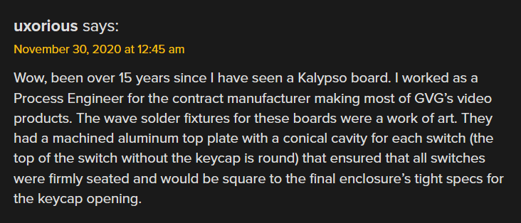
Wow, been over 15 years since I have seen a Kalypso board. I worked as a Process Engineer for the contract manufacturer making most of GVG’s video products. The wave solder fixtures for these boards were a work of art. They had a machined aluminum top plate with a conical cavity for each switch (the top of the switch without the keycap is round) that ensured that all switches were firmly seated and would be square to the final enclosure’s tight specs for the keycap opening.
It was pretty cool to hear some of the history from someone involved in the manufacture of these panels. I can confirm that the switches are round underneath their caps:
The switches are indeed round underneath their caps.
And the tolerances are pretty tight too:
Not much of a gap between the keys and the enclosure on this Grass Valley Group Kalypso 1-M/E panel.
-Glen