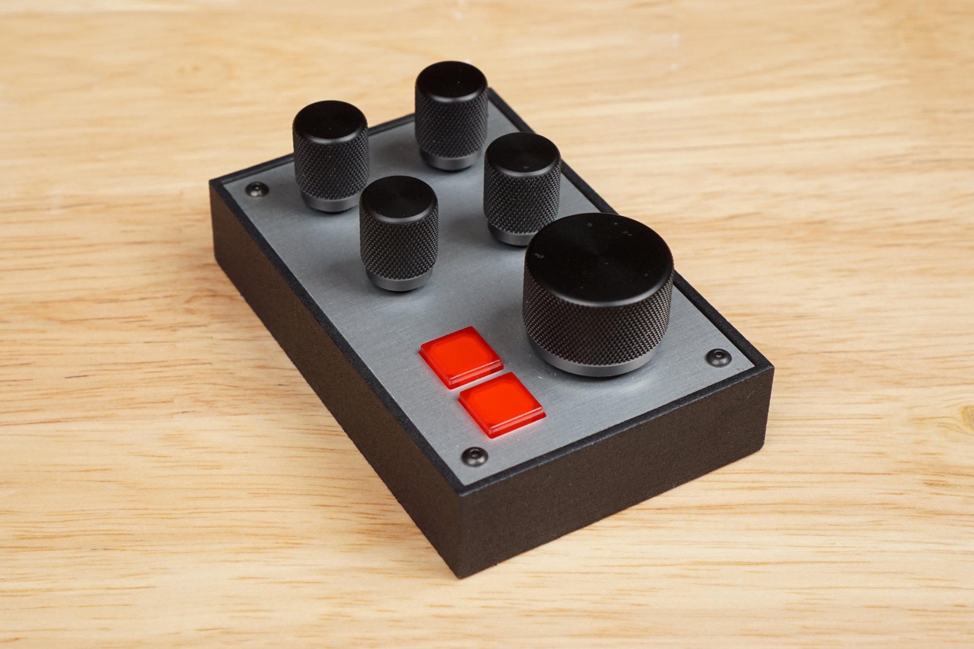
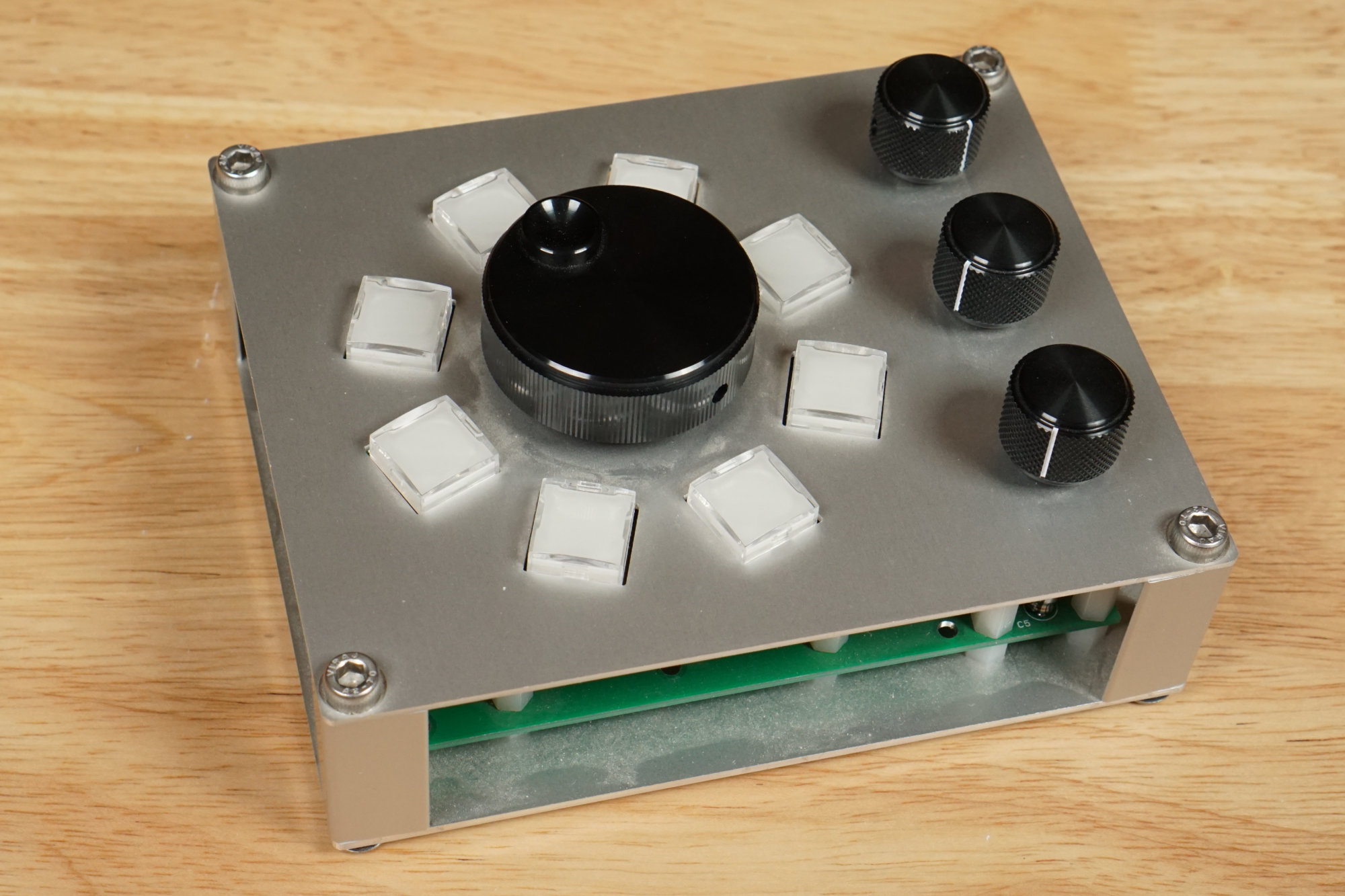
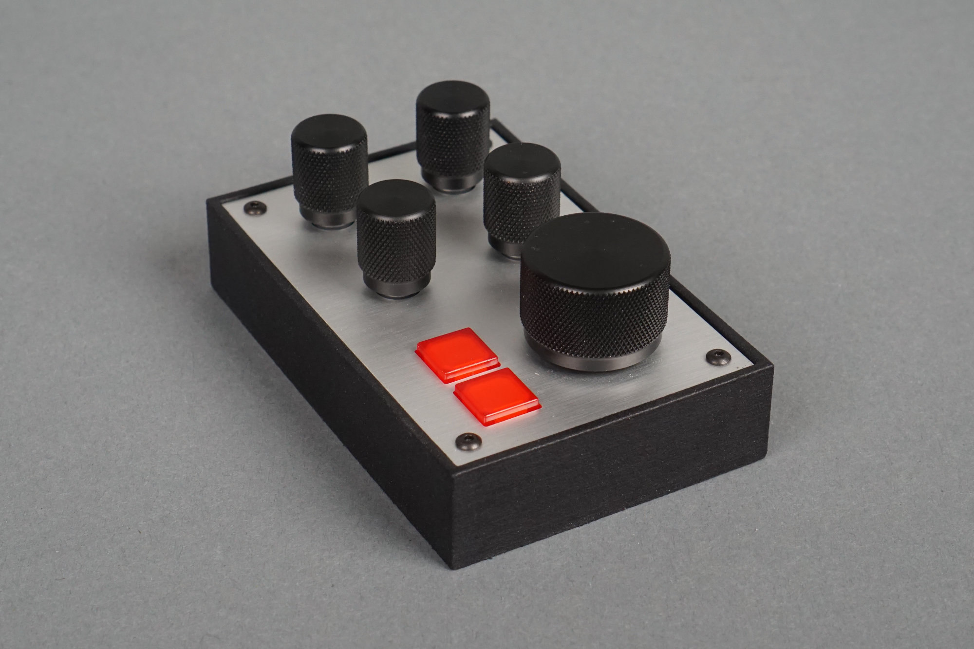
The finished USB Knob Box.
I have a Blackmagic Designs Micro Studio Camera I wanted to use as a webcam for video conferences. Even with a 16mm sensor, it has better quality than any small sensor webcam. The only issue is all the exposure and focus controls are manual. When connected to one of their ATEM video switchers, this isn’t a problem as the ATEM provides control of all connected cameras using data sent back to the camera embedded in the HD-SDI return video feed.
If you want to use the camera without an ATEM swtich, however, there’s no way to control the exposure without using the small awkward buttons on the front of the camera and no way to control the focus without reaching up and turning the lens’s focus ring. Being an engineer, hacker, and maker, there had to be a better way! And there was. Read on to find out more about my solution for controlling the camera. Also, it’s 100% open source and licensed under the permissive MIT license if you want to build your own.
Blackmagic Designs Micro Studio Camera 4K Control
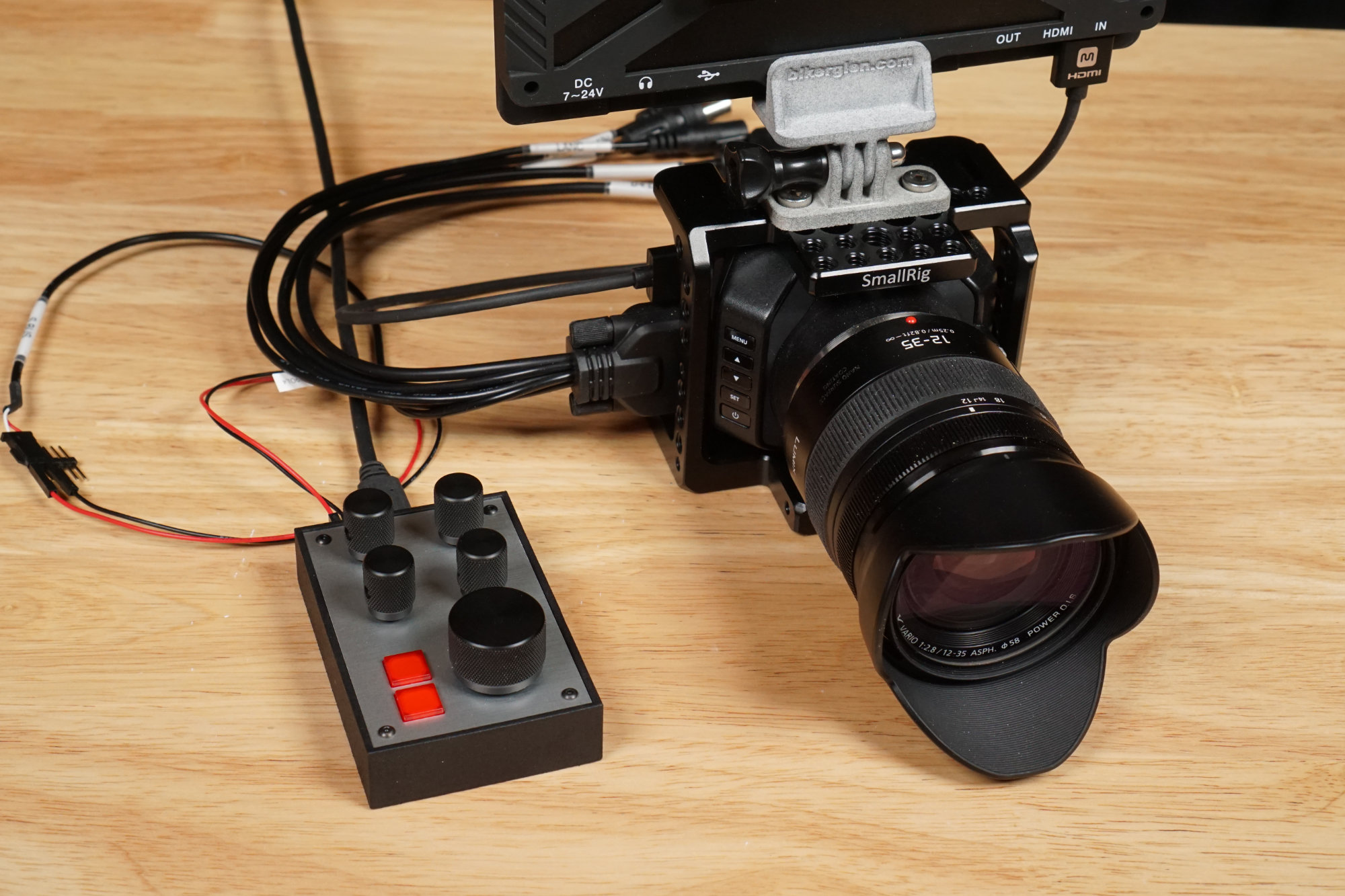
The finished project connected to and controlling a Blackmagic Designs Micro Studio Camera 4K.
The Blackmagic Designs Micro Studio Camera is designed to be remote controlled. They have a huge section dedicated to remote control on the camera’s webpage. The three methods of controlling the camera and connected lenses are through the HD-SDI return video feed, using the LANC port, or using the S.BUS port.
Control using the HD-SDI Return Video Feed
The primary method of controlling the camera exposure and lens zoom and focus is using the HD-SDI return video feed. The HD-SDI return video feed connects from the ATEM switcher back to the camera. It sends program video, program audio, intercom audio, tally light, and camera control data from the switcher back to the camera.
All the ATEM switcher products have a camera control unit (CCU) panel in their control software. The CCU panel permits adjusting the camera white balance, color, and exposure and controlling the zoom and focus on supported lenses. The ATEM switcher encodes and embeds the camera and lens adjustments into the return video feed sent back to the camera.
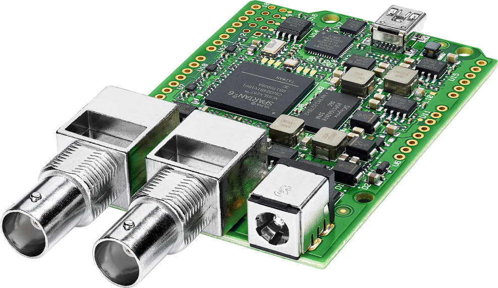
The Blackmagic 3G-SDI Shield for Arduino. Image stolen from the BMD website.
Blackmagic Design also makes an Arduino shield that supports sending a subset of this data to the camera. The shield has an HD-SDI video input, an HD-SDI video output, an I2C interface, and an Arduino library. The shield connects to an Arduino then the Arduino library can be used to send camera and lense control commands over I2C to the shield which embeds them into the HD-SDI output for transmission to the camera.
This is a really cool control scheme and lets users control everything from an embedded system that you could normally control through the ATEM CCU panel. Unfortunately the Arduino shields are $99 and usually backordered. I am going to build a controller based on the Arduino shield someday but not right now.
Control using the LANC Port
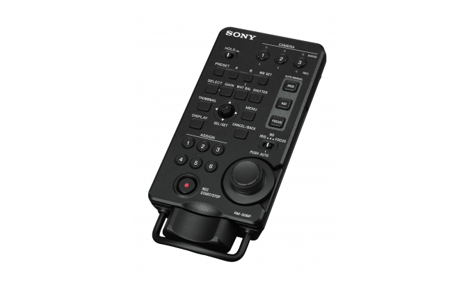
The ridiculously expensive Sony RM-30BP wired LANC remote control. $925. Ouch. Just no.
The second way to control the exposure and the lens is using the LANC protocol on the camera’s expansion port. Most LANC controllers are designed to mount to a tripod and permit the camera operator to control the lens without having to reach to the front of the camera. The only controller that seemed suitable to me was one made by Sony that was $925 and there was no telling how well (or not) it would work with a Blackmagic camera with a Panasonic lens. The rest would take up too much space on my desk or only control a subset of the camera’s functions.
Control using the S.BUS Protocol
The final way to control the exposure and the lens is using the Futaba S.BUS protocol. The S.BUS protocol is a digital protocol used by radio-controlled cars, trucks, and aircraft. The protocol links radio receivers to one or more servo motors in the model.
The Blackmagic Micro Studio Camera is small enough that one target market is drone photography and videography. Using the S.BUS protocol, the camera could connect to the existing radio receiver on the drone and permit an operator on the ground to adjust the camera and lens using their existing radio equipment.
The S.BUS protocol is proprietary but it’s been reverse engineered. A good reference with example code can be found on Github. It’s basically inverted TTL-level serial data at 100 kbps with even parity and two stop bits. 16 channels of 11 bits are mapped into 25 data bytes that are sent over the serial link.
The only really complicated part is mapping the 16 channels of 11 bits into 25 bytes of 8 bits correctly. I used the servo channel packing code from BMC_SBUS.cpp file in the aforementioned repository. The Studio Micro Camera manual contains a brief section on mapping camera and lens control data into servo channels. This was the approach I decided to take.
Early Knob Box Experiments
My first box of knobs and buttons from 2012.
I decided I wanted a box with lots and lots of knobs to control the camera. I looked around the house to see if I had already built anything similar and I found the knob box pictured above. This was my first attempt at building a knob box back in 2012. It was roughly inspired by Sun Microsystems’s SunDials and video editor jog / shuttle controls. It was based on a PIC24 and had a serial connection to a PC for reporting knob turns and buttons presses and receiving commands to control the lights in the pushbuttons.
Six boards?
It’s rather complicated with six circuit boards and multiple levels of components. It was designed without the use of any mechanical / 3D CAD software and, frankly, I’m surprised it came together as well as it did. I never bothered to get the side panels cut. It was also too big relative to the amount of free space on my desk to meet my current needs.
I did change the software to verify I could use a few of the knobs to control the camera from the PIC24 micro on the main board. This worked for a proof of concept, but I needed something smaller, less expensive, and easier to assemble.
Design Requirements
After surveying the available ATEM, LANC, and S.BUS controller products and looking through my existing projects, I decided I needed to build a new more modern knob box to use to control the camera. The design requirements were:
- Build a small box with direct control of most camera and lens functions.
- Use the S.BUS protocol to control the camera and lens.
- Must be capable of controlling white balance, gain, shutter, iris, focus, and zoom (if supported by the lens).
- Capable of using a USB bootloader to install firmware updates. This negates the need for dedicated programming hardware and permits the device to be updated without disassembly.
- Vendor-defined USB HID functionality would be nice to have.
- Use a 3D printed enclosure.
- Use an aluminum front panel.
- Low cost thus ruling out the use of pricey optical encoders.
Schematic Design
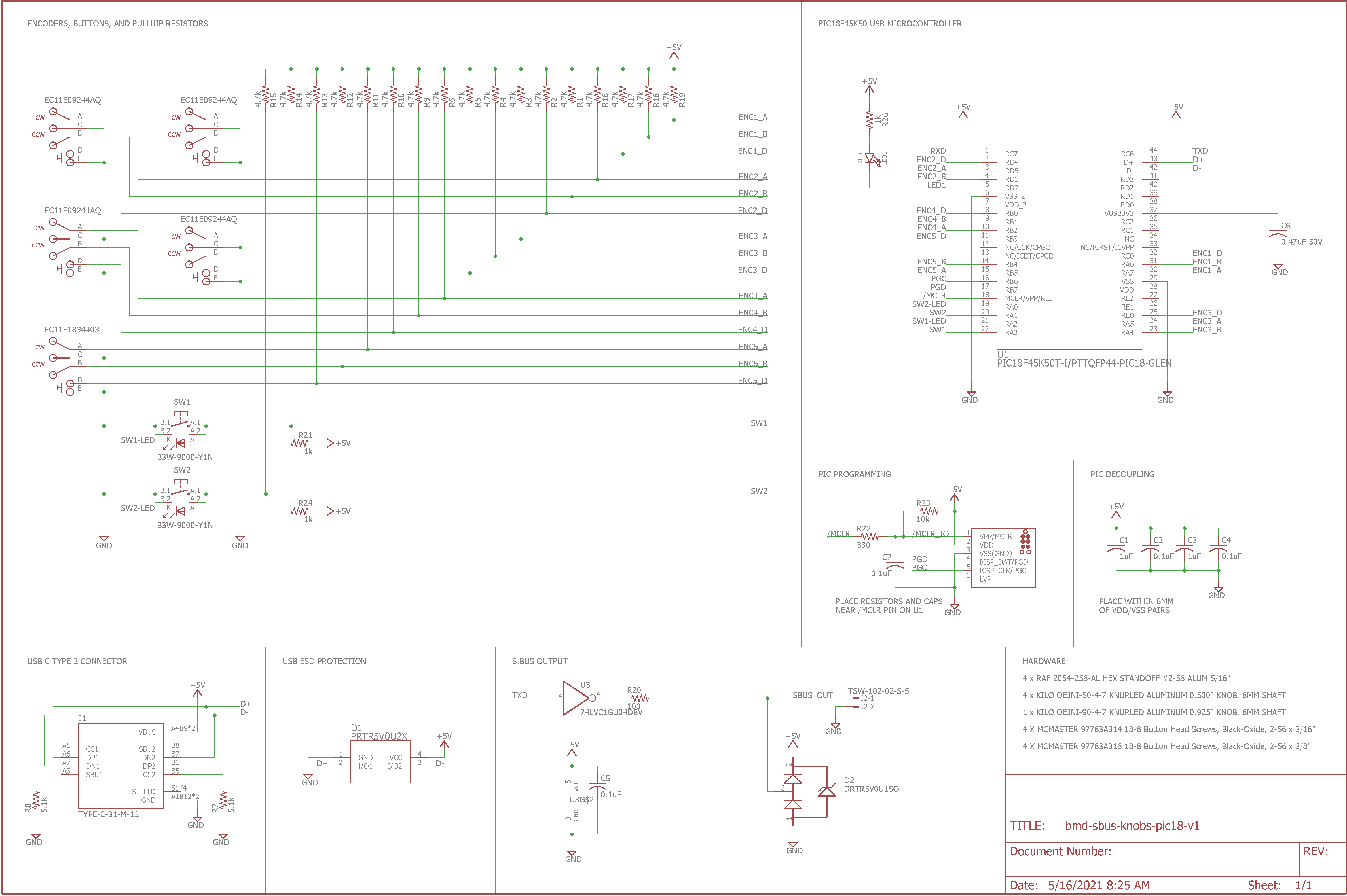
The complete schematic for the project.
With the requirements out of the way, it was time to turn to the schematic. The complete schematic is shown above. Let’s examine each section of the schematic separately.
PIC18F45K50 Minimum Circuit
The PIC18F45K50 minimum circuit consists of the PIC18F45K50 USB microcontroller, PIC programming, and PIC decoupling sections of the schematic. I’m using the five-volt version of the part so C6 is necessary for stable operation of the on-board 3.3 volt regulator.
The PIC programming section consists of a programming connector and a filtering circuit to prevent inadvertent device resets. In this case, I’m using a TAG-Connect programming cable so the programming connector consists of six pads and three holes to accommodate the cable’s POGO pins.
The PIC decoupling section is the required decoupling for the part. The 1 uF capacitors, C1 and C3, are only necessary because the PIC is located at the end of a long USB cable that supplies the 5 volt operating voltage for the part. If the PIC was on the same board as the 5 volt power supply, the 1 uF capacitors would likely not be necessary.
LED1 and R26, while not strictly necessary, are a nice to have during bring up. No crystal or oscillator is necessary as the PIC will be running from its internal oscillator and active clock tuning will be enabled to keep the clock within USB’s specs while operating as a USB device.
USB
USB functionality is built into the PIC18F45K50. The only required components are the USB connector and ESD protection on the USB lines. These are shown in the USB C Type 2 connector and USB ESD protection sections of the schematic. The 5.1k resistors, R7 and R8, are necessary for proper enumeration of the knob box when connected to a real USB C port on a computer.
Encoders
I chose two different encoders for this project. Both are from the ALPS EC11 family with flatted 6 mm D shafts. The first encoder type is for settings that have coarse adjustments. There are four of these encoders. They are used to control white balance, gain, shutter speed, and iris. These encoders have 18 detents and 9 pulses per revolution.
The second encoder type is the for settings that have fine adjustments. There is one of these encoders. It is used to control focus. This encoder has no detents and generates 18 pulses per revolution. Unlike the $30 to $60 optical encoders I’ve used on previous projects, these mechanical encoders are only about $5 each.
All the encoders have switches. Both the encoder wheel contacts and encoder switch contacts require 4.7k pullup resistors to the five volt supply rail.
Buttons
I added two buttons to the project. These buttons are basic tactile normally-open pushbutton switches with internal LEDs for illumination and bright red lens caps. The switches use 4.7k pullup resistors and the LEDs use 1k series current limiting resistors.
The buttons serve two purposes. First, if the top button is pressed during power up, the knob box enters USB bootloader mode enabling the knob box software to be updated from a PC. Second, the top button is used to switch between using the big knob to adjust lens focus and using the big knob to adjust lens zoom. (Both bootloader and focus/zoom select are future features that were not implemented when this post was written.)
The bottom button is not used.
S.BUS Output
The S.BUS output section of the schematic shows the hardware required for the S.BUS output. There’s an inverter to invert the serial output from the PIC. The inverter is not strictly necessary since the PIC can invert its serial output internally based on a register bit but it does provide some isolation between the exposed S.BUS output port and the PIC. The inverter has a decoupling cap. There’s also a 100 ohm resistor and an ESD suppression diode on the output line to protect the PIC from ESD and noise.
Hardware
I frequently build things then can’t remember what screws, knobs, nuts, and bolts I used on the project. To prevent that on this project, I added a hardware section in the lower right hand corner of the schematic that lists all the hardware needed for this project.
Board Design
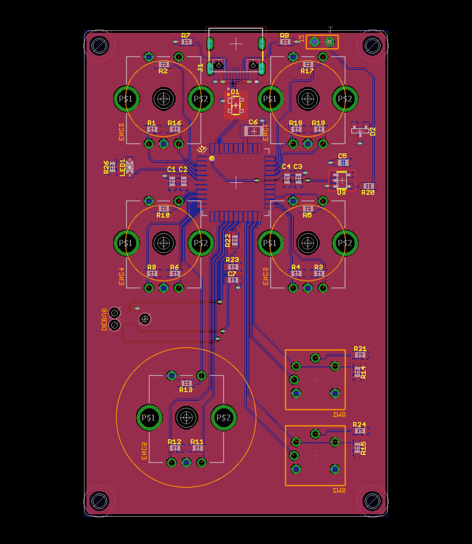
The completed board design.
The toughest part of the board design was deciding on the spacing and location of the encoders and buttons. Once I decided on a decent layout for these components, I placed them on the bottom of the board then placed the PIC and most of the remaining components on the top of the board. The diameters of the knobs and the locations of the buttons are indicated in orange which is the bottom silkscreen layer.
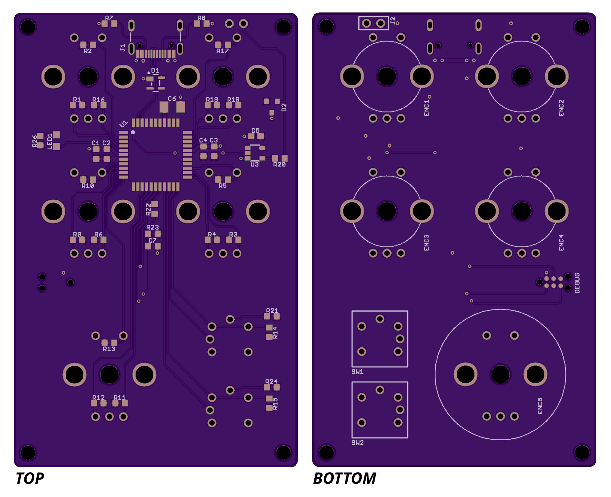
OSH Park’s preview of the boards.
After designing the board, I uploaded it to OSH Park’s website and looked over the preview. The preview of the bottom of the board is shown as though you were holding the board in your hand so the buttons are in the lower-left which is where they should be. The preview looked good so I ordered boards.
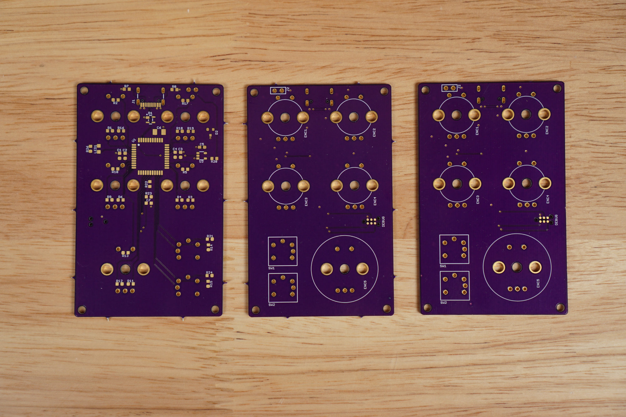
The finished boards. I used a rotary tool with a grinder bit to file off the mouse bites on the far right board.
About two weeks later, I received the finished boards which are pictured above. Left to right are the top of the first board, the bottom of the second board, and the bottom of the third board. On the third board, I used a rotary tool with a grinding bit to grind off the mouse bites. This is the board I assembled for the project.
Enclosure Design
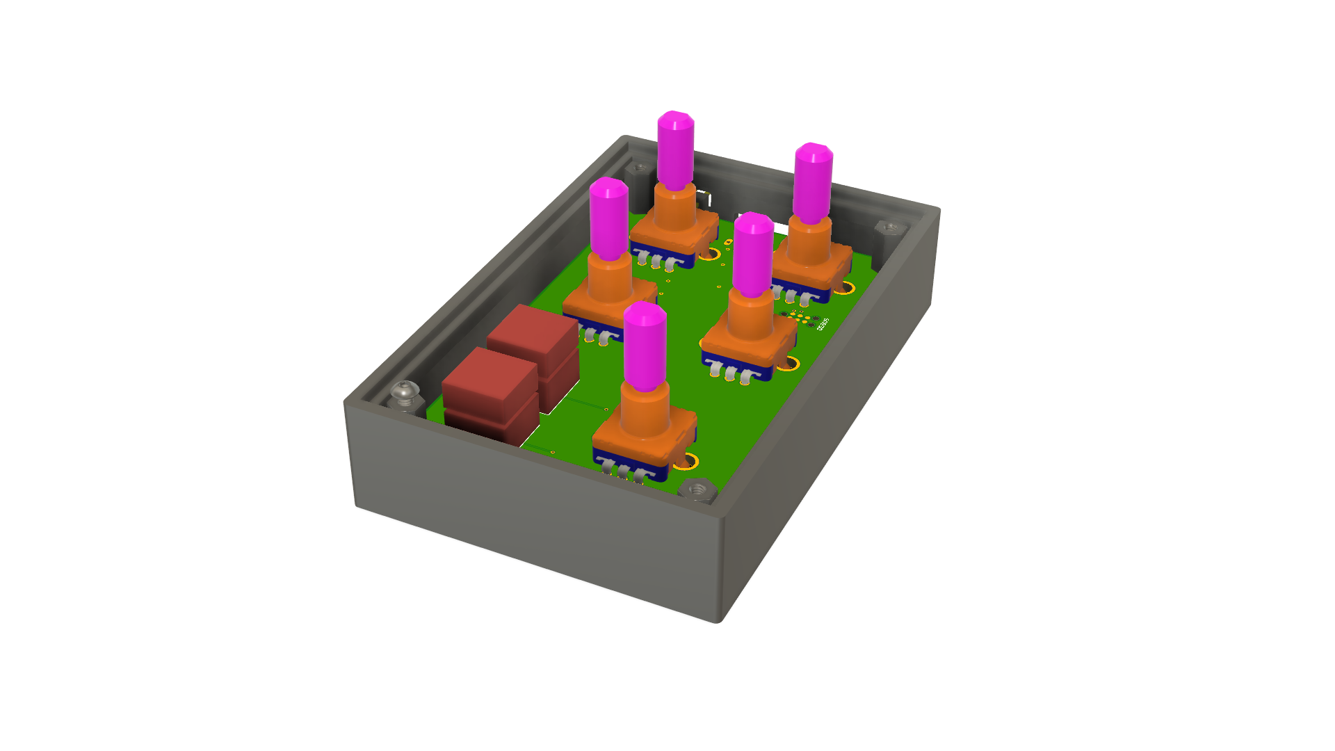
The enclosure design with the circuit board, knobs, buttons, and connectors.
I designed the enclosure in Fusion 360. Once the enclosure was designed I imported the circuit board from Eagle and placed it in the enclosure to check fit. I also imported the top panel (shown the next section) and checked its fit.
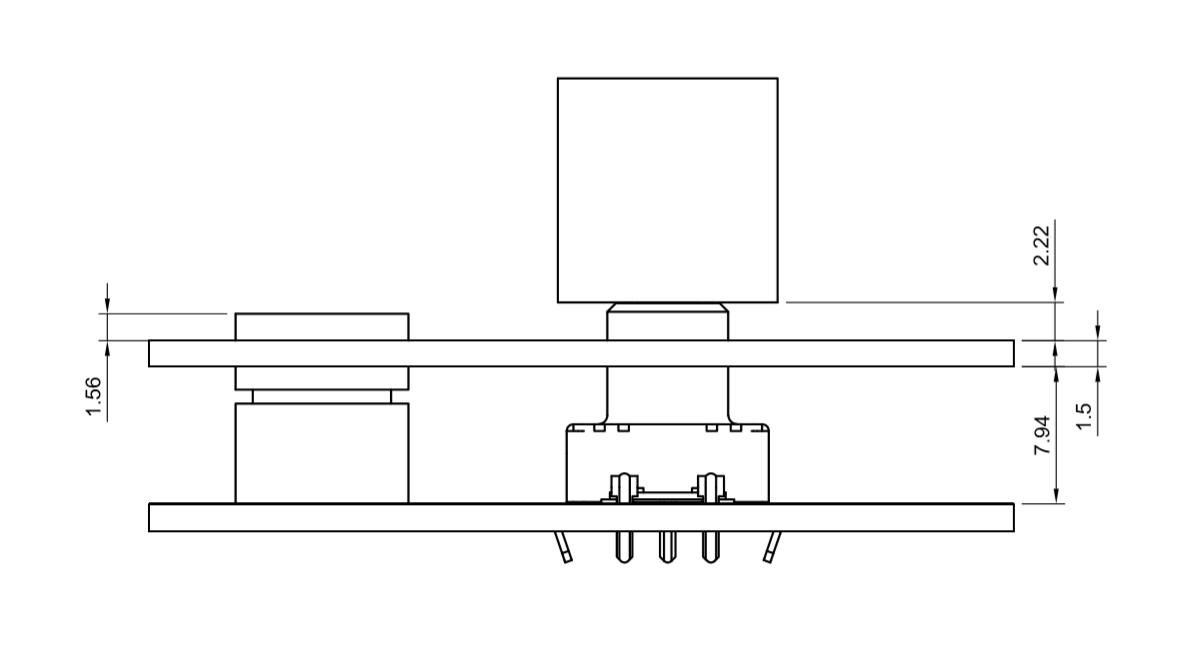
A quick drawing showing the knobs will have plenty of clearance when pressed to avoid hitting the aluminum panel.
The most important interference check was making sure the knobs could be pressed without hitting the lid of the enclosure. The diagram above shows there’s plenty of clearance for the knobs 1.5mm travel without hitting the panel. Everything looked good so I used Sculpeo’s 3D printing service to 3D print the enclosure.
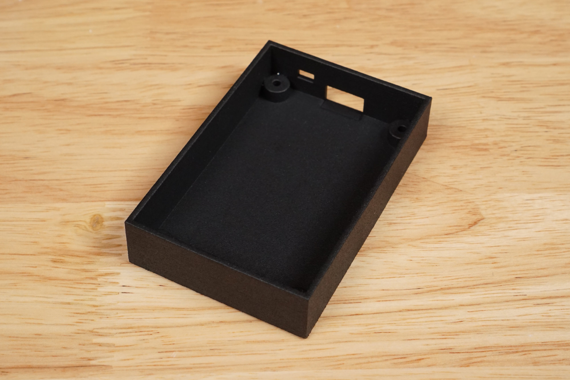
The empty 3D printed enclosure.
I used Scultpeo’s HP Multi Jet Fusion process to 3D print the enclosure. I then had them dye the enclosure solid black. There’s supposed to be a thin lip around the top of the enclosure to keep the front panel from falling inside the enclosure but it looks like it might have been too thin and either didn’t print or broke off during the finishing process. The thin lip was really more for aesthetics than functionality so the enclosure is usable even without it.
Front Panel Design
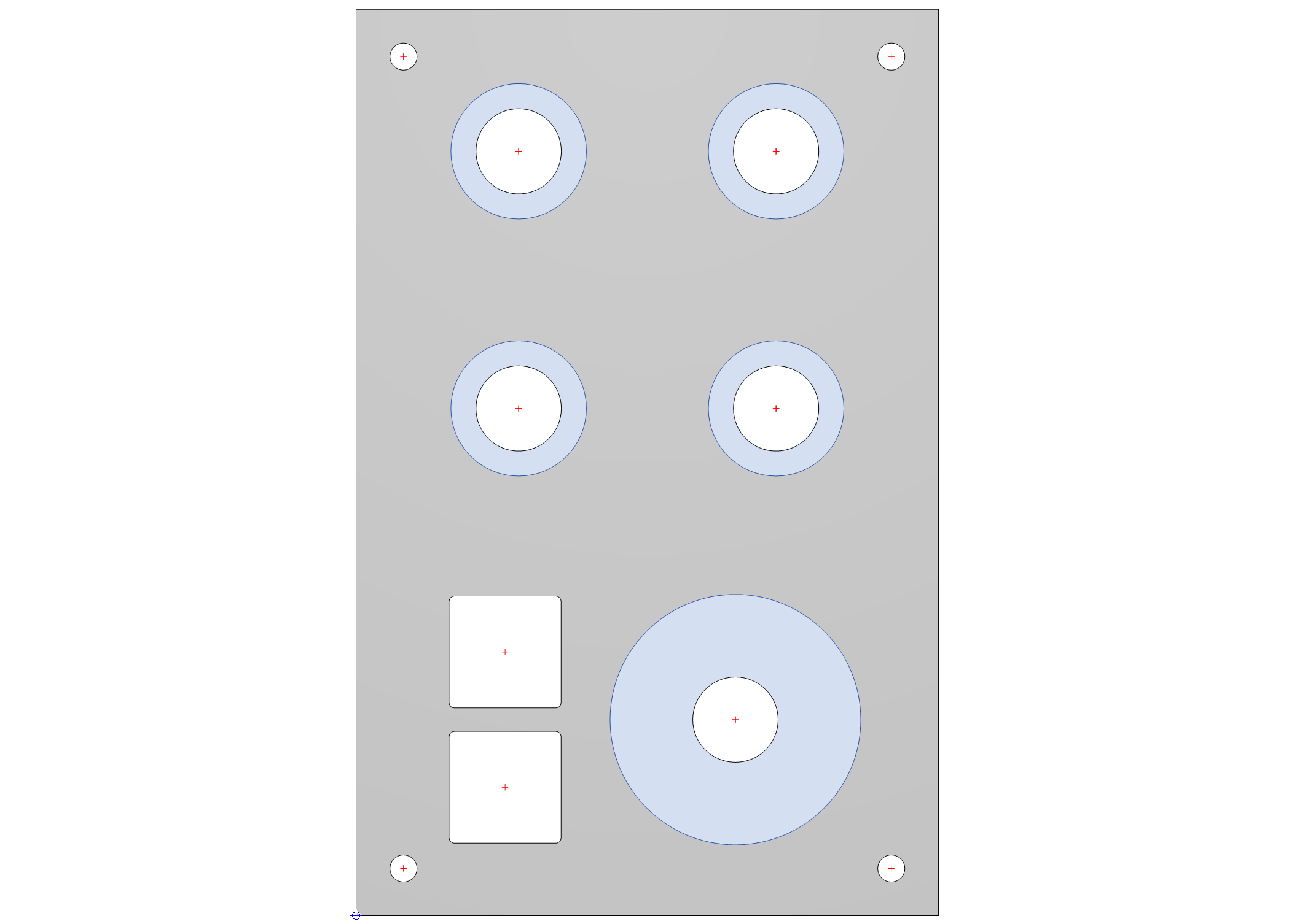
The completed front panel. The area occupied by the knobs is shown in blue.
I used Front Panel Express’s Front Panel Designer software to design the front panel for the project. The front panel fits within the enclosure and is held above the board by 2-56 x 5/16″ threaded spacers.

Testing for interference in Fusion 360 before ordering the boards, panels, and enclosure.
Once the lid was designed, I exported as a DXF file and imported it into Fusion 360 to verify it fit correctly. It did so I ordered the lid. I also ordered a second lid in red for kicks since I’ll likely build two of these. The red anodized lid is 2 mm thick instead of 1.5 mm thick like the clear anodized lid so a 0.5 mm washer must be inserted into each knob to keep them from hitting the red panel.
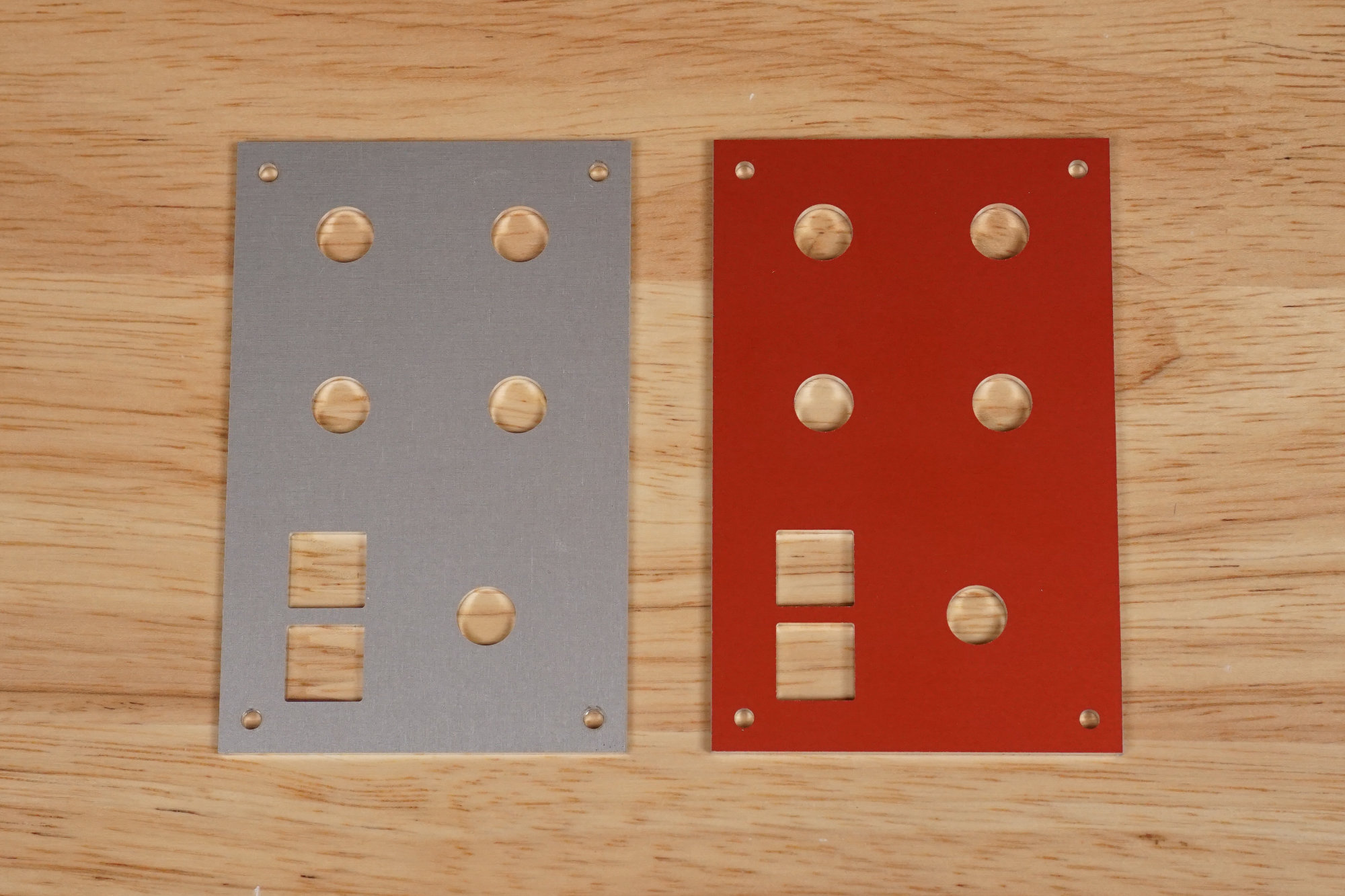
The CNC’ed front panels. I had an extra panel cut out of red anodized aluminum.
The finished panels are shown in the photo above. Later I might order another lid with the functions of the knobs etched into the panel and highlighted in black paint (if clear anodized aluminum) or white paint (if red anodized aluminum).
Embedded Software
Development While Waiting on Boards and Parts
Initial software development was done with an eval board and a knob board leftover from the original bulky knob box project.
I decided to start the software while waiting on boards. To do this, I ordered the only Microchip evaluation board that I could find with a PIC18F45K50 device. The Microchip Library for Applications contains a vendor-defined USB HID example for this board. I was able to use that code as a starting point for my software. I was able to do quite a bit with the eval board while waiting for my real boards.
Once I got the example code up and running, I started modifying it for my application. The first thing I did was get timer 2 running at 250 Hz to serve as the heartbeat for the software.
Using the timer, I was able to blink the leftmost LED on the eval board. I then modified the code to blink different patterns based on the USB state: 1 blink every 1.5 seconds = USB not connected; 2 blinks = connected but not fully enumerated; 3 blinks = connected and running. This LED would eventually be replaced by the “blinky” red LED on the bottom of the board.
The next step was to control the next two LEDs on the eval board over USB. These LEDs would eventually be replaced by the LEDs built into the two switches on the top of the board. I modified the MLA USB descriptors and MLA USB code and was able to control the two LEDs over USB from either Windows or Linux.
The eval board has two user-defined buttons. The next step was to report these keys being pressed or released to the USB host. These buttons would later be replaced by the two red buttons on the top of the real boards.
Going back to my original knob box from 2012, I remembered having some extra boards. I eventually found a blank, unstuffed board from this project and an extra encoder. I soldered the encoder and required pullup resistors to the board, found some unused GPIO pins on the PIC on the eval board, then connected the knob board to the eval board. Using this setup, I was able to write the software required to report knob turns and knob presses to the PC.
Using the eval board, I was able to develop a known good version of the code that supported the USB, buttons, LEDs, and encoders on my real board. This known good code would be useful for bringing up the real boards.
Board Bring-Up

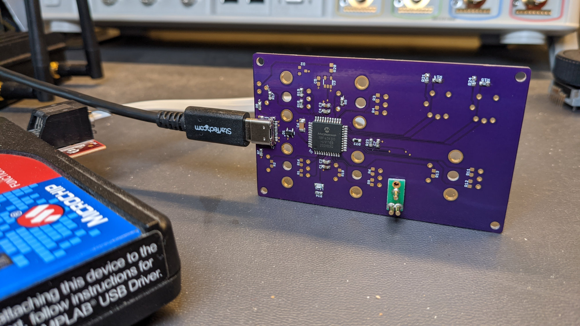
Just enough components to verify the PIC, debugger, and USB are working.
When the real boards arrived, I stuffed just enough components to verify I could program the PIC, the PIC would run, and USB would work. I also stuffed a red LED on the bottom of the board to blink. I left off the encoders, buttons, most of the pullup resistors, and the S.BUS output parts for now.
Trying the initial build of the software with none of the controls installed.
Initially I ran the eval board software completely unmodified on the real boards. This was enough to prove the PIC could be programmed, the PIC ran, and USB worked. Once this step was completed, I slowly started changing defines in one of the header files to point at my real hardware rather than the eval board hardware. First the red “blinky” led. Build, program, test.
Once the blinky LED was verified as functional, I stuffed both buttons and one knob, changed the defines, compiled, programmed, and tested again. These worked too. At this point I was satisfied that there were no large errors in the board design so I finished stuffing the board.
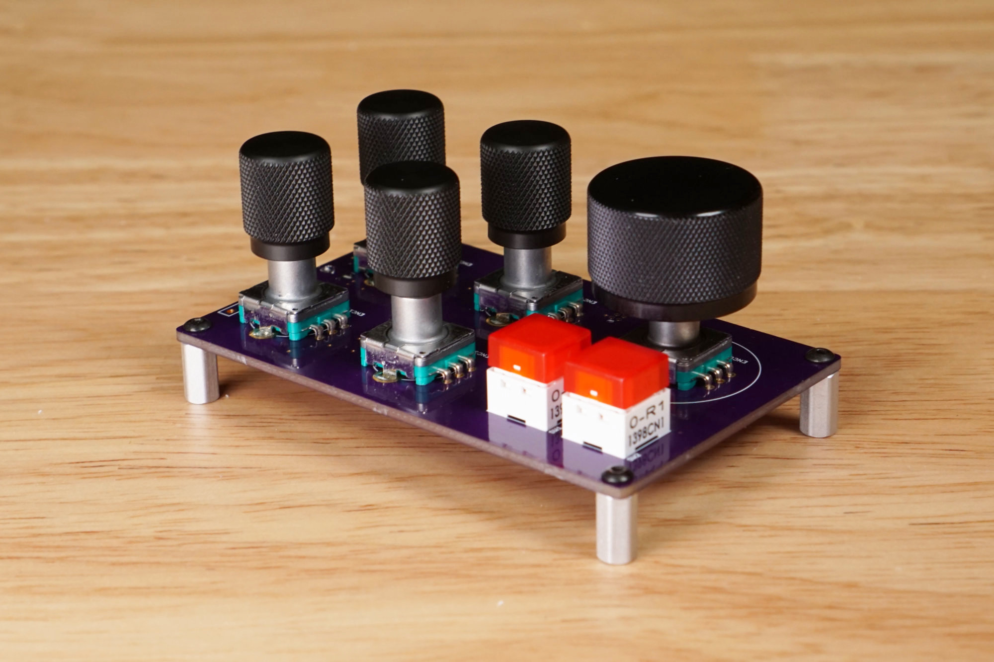
Once the PIC, debugger, and USB were verified, I added the knobs and buttons.
I tested the remaining hardware. I found one solder bridge between the S.BUS output and ground which was an easy fix. Let’s take a closer look at the key parts of the software.
Reading Encoders
Fundamentally, this project is all about the knobs so the knobs need to function flawlessly. Getting flawless operation started with reading the data sheet. The three biggest takeaways from the data sheet were:
- The knobs have a chattering as they’re turned of up to 3 ms. We need to read the knobs as quickly as possible so as not to miss any pulses but if we read them faster than about every three milliseconds, we’re going to see noise as the knob rotates through each pulse. We also need to filter out the chattering.
- The buttons in the knobs have a bounce of up to 2 ms. It’s hard if not impossible to for a user to press and release the keys every 2 ms but we should still sample them relatively quickly and filter out the bouncing.
- “Detent stability position cannot be specified for the B signal” What??? This means that on the knobs with detents, the B signal is of unknown value when the knob is resting in a detent. We need to use A signal to detect motion then sample the B signal to determine the knob direction.
Based on the above notes, I settled on a sampling period of 4 ms / a sampling frequency of 250 Hz. This is why the timer 2 main loop timer is running at 250 Hz.
To read the encoders, I specify the encoder pins:
// encoder pins
#define ENC1_A   (PORTAbits.RA7 ? 1 : 0)
#define ENC1_B   (PORTAbits.RA6 ? 1 : 0)
I declare some global variables to hold their states:
// encoder states
uint8_t enc1a;
uint8_t enc1b;
Then every 4 ms I sample the encoders and get their direction based on the current sample and the last two samples of both the A and B pins:
// sample encoders
enc1a = ((enc1a << 1) | ENC1_A) & 7;
enc1b = ((enc1b << 1) | ENC1_B) & 7;

// process encoders
thisUsbReportData[1] = GetDirection (enc1a, enc1b);
The GetDirection function does the heavy lifting:
uint8_t GetDirection (uint8_t a, uint8_t b)
{
    if (a == 4) {
        // 100 => falling edge
        return (b & 2) ? 0x01 : 0x02; // 0x01 = cw, 0x02 = ccw
    } else if (a == 3) {
        // 011 => rising edge
        return (b & 2) ? 0x02 : 0x01; // 0x02 = ccw, 0x01 = cw
    }

    return 0;
}
This function returns 0 for no change, 1 for a CW click, and 2 for a CCW click. If the return value is non-zero, the direction CW or CCW is reported to the USB host and the one of the camera parameters are updated over the S.BUS output. If the return value is zero, no further action needs to be taken for this encoder. This sampling and processing is repeated for the remaining four encoders.
Reading Buttons
The buttons embedded into the knobs as well as the two pushbutton switches are noisy and need to be debounced too. The basic procedure is to report a button as pressed only if it reads pressed on two consecutive samples and report a button as released only if it reads released on two consecutive samples.
I specify the button pins:
// define buttons
#define ENC1_SW  (PORTCbits.RC0 ? 0 : 1)
#define ENC2_SW  (PORTDbits.RD4 ? 0 : 1)
#define ENC3_SW  (PORTEbits.RE0 ? 0 : 1)
#define ENC4_SW  (PORTBbits.RB0 ? 0 : 1)
#define ENC5_SW  (PORTBbits.RB3 ? 0 : 1)
#define SW1      (PORTAbits.RA3 ? 0 : 1)
#define SW2      (PORTAbits.RA1 ? 0 : 1)
I declare a global variable to hold their states:
// button debounce states
uint8_t buttonStates[8];
Every 4 ms, I sample all the buttons (five knob buttons and two switch buttons) and update their states:
// sample and process buttons
thisUsbReportData[0] |= ProcessButton (0, ENC1_SW);
thisUsbReportData[0] |= ProcessButton (1, ENC2_SW);
thisUsbReportData[0] |= ProcessButton (2, ENC3_SW);
thisUsbReportData[0] |= ProcessButton (3, ENC4_SW);
thisUsbReportData[0] |= ProcessButton (4, ENC5_SW);
thisUsbReportData[0] |= ProcessButton (5, SW1);
thisUsbReportData[0] |= ProcessButton (6, SW2);
The ProcessButton function does the heavy lifting:
uint8_t ProcessButton (uint8_t which, uint8_t sw)
{
    uint8_t state;

    state = buttonStates[which];

    switch (state) {
        case 0: state = sw ? 1 : 0; break;
        case 1: state = sw ? 2 : 0; break;
        case 2: state = sw ? 2 : 3; break;
        case 3: state = sw ? 2 : 0; break;
    }

    buttonStates[which] = state;

    return (state & 2) ? (1 << which) : 0;
}
The button states are only sent to the USB host if different buttons are pressed this time around the main loop versus the last time around the main loop.
Sending Data over USB
Data is sent over USB using a modified version of the APP_DeviceCustomnHIDTasks function from the MLA code. This code sees if a report is needed and if the IN endpoint is free. If a report is needed and the endpoint is free, a report is sent from the device to the host. The report is formatted according to the USB report descriptor for report ID 1.
if (usbReportNeeded) {
    if (!HIDTxHandleBusy(USBInHandle)) {
        usbReportNeeded = false;
        ToSendDataBuffer[0] = 0x01; // report ID
        ToSendDataBuffer[1] = usbReportData[0];
        ToSendDataBuffer[2] = usbReportData[1];
        ToSendDataBuffer[3] = usbReportData[2];
        ToSendDataBuffer[4] = usbReportData[3];
        ToSendDataBuffer[5] = usbReportData[4];
        ToSendDataBuffer[6] = usbReportData[5];
        //Prepare the USB module to send the data packet to the host
        USBInHandle = HIDTxPacket(CUSTOM_DEVICE_HID_EP, (uint8_t*)&ToSendDataBuffer[0],7);
    }
}
Receiving Data over USB
The APP_DeviceCustomnHIDTasks function from the MLA code also receives data over USB. This code sees if the OUT endpoint is no longer busy and if the report ID matches the report ID from the USB report descriptor. If it does, the LEDs embedded in the pushbutton switches are turned on or off based on the data in the body of the OUT report.
//Check if we have received an OUT data packet from the host
if(HIDRxHandleBusy(USBOutHandle) == false)
{
    // check report ID
    if (ReceivedDataBuffer[0] == 2) {
        if (ReceivedDataBuffer[1] & 1) {
            SW1_LED = LED_ON;
        } else {
            SW1_LED = LED_OFF;
        }
        if (ReceivedDataBuffer[1] & 2) {
            SW2_LED = LED_ON;
        } else {
            SW2_LED = LED_OFF;
        }
    }

    //Re-arm the OUT endpoint, so we can receive the next OUT data packet
    //that the host may try to send us.
    USBOutHandle = HIDRxPacket(CUSTOM_DEVICE_HID_EP, (uint8_t*)&ReceivedDataBuffer[0], 64);
}
Sending Data to the BMD Camera
Data is sent to the BMD camera according to the instructions in the camera manual and formatted according to the S.BUS protocol. White balance, gain, and shutter speed are “stick up / stick down” parameters while iris, zoom, and focus are “stick position” parameters.
Stick Up, Stick Down
Think of a radio control transmitter with a stick that is normally centered. White balance, gain, and shutter speed are adjusted by pressing the normally centered control stick up to increase their value or down to decrease their value. The knob box software needs to mimic the behavior of the stick on the radio control transmitter.
A centered stick corresponds to the middle of the servo channel value range with a value of 128, stick up is 212, and stick down is 44. For each increment of a parameter, the stick needs to start at its centered value, go to the stick up value, then go back down to the centered value before it can go up again or go down. For this reason the knob software counts the clicks the knobs are turned then sends a stick up, stick centered or stick down, stick centered sequence and decrements the knob click count after sending each sequence. The result is no knob clicks are missed.
Stick Position
Iris, zoom, and focus function differently than white balance, gain, and shutter speed. These are stick position parameters. Again think of the radio control transmitter. This time the stick stays where the operator placed it. Moving the stick up opens the iris while moving the stick down closes the iris. When the operator releases the stick, it stays in place and so does the iris. Zoom and focus operate similarly.
The software mimics this behavior by constantly sending an absolute value between 44 and 212 based on tracking the total number of times the knob has been clicked CW or CCW since reset.
Servo Channel Data
S.BUS supports 16 channels of 11 bits each. The camera control parameters are mapped into channels using a collection of defines at the beginning of main.c:
// servo channel mappings
#define IRIS_CHANNEL          1
#define FOCUS_CHANNEL         2
#define AUTOFOCUS_CHANNEL     3
#define GAIN_CHANNEL          5
#define SHUTTER_CHANNEL       6
#define WHITE_BALANCE_CHANNEL 7
These need to be set the same as the S.BUS servo channels in the setup menu on the camera. These use a zero-indexed numbering scheme. The camera uses a one-indexed numbering scheme. Channel 1 in the define above corresponds to channel 2 on the camera and so on.
Each channel is 11 bits. The BMD camera only uses the upper 8 bits so really the maximum of 212 is (212 << 3), the mid range of 128 is (128 << 3), and the lower limit of 44 is really (44 << 3).
S.BUS Data Transmission
Every three times around the main loop, the servo channel values are mapped into their S.BUS data bytes and output on EUSART1. 25 bytes are transmitted every 12 ms.
The S.BUS protocol runs at 100 kbps with even parity and two stop bits. This particular PIC18 doesn’t support parity or stop bits. It has a nine-bit data mode that can be used to mimic a parity bit or a second stop bit but not a parity bit and an additional stop bit at the same time. And I checked. The BMD camera really does require even parity and two stop bits; one stop bit alone is not sufficient for reliable operation. Grrr.
To workaround this, I use the nine-bit data mode to transmit even parity and I use timer 0 to time the sending of bytes out the serial port. Basically timer 0 is set to expire after 12 bit times (start bit + 8 data bits + parity bit + two stop bits). When the the first 11 bits are done being sent, the TX output on the PIC goes high but the timer prevents data from being transmitted for an additional bit time. This mimics a second stop bit. It’s not exact but it works.
Once the S.BUS transmit data array is loaded, the main loop executes the following code to kick off a series of timer interrupts that transmit the S.BUS data:
// send sbus data to camera
txByte = 0;
TMR0H = TMR0_RELOAD_VALUE >> 8;
TMR0L = TMR0_RELOAD_VALUE & 0xFF;
INTCONbits.TMR0IF = 0;
INTCONbits.TMR0IE = 1;
TIMER_RELOAD_VALUE corresponds to 12 bit times at 100 kbps or 120 us. The ISR code that transmits the 25 bytes looks like this:
if (INTCONbits.TMR0IE == 1 && INTCONbits.TMR0IF == 1)
{
    TMR0H = TMR0_RELOAD_VALUE >> 8;
    TMR0L = TMR0_RELOAD_VALUE & 0xFF;
    INTCONbits.TMR0IF = 0;

    x = sbusData[txByte++];
    y = x ^ (x >> 4);
    y = y ^ (y >> 2);
    y = y ^ (y >> 1);
    TXSTA1bits.TX9D = y & 1;
    TXREG1 = x;

    if (txByte >= 25) {
        INTCONbits.TMR0IE = 0;
    }
}
Hopefully, Microchip will release a PIC18 device that supports USB, active clock tuning, and a UART with parity and two stop bits at some point.
Assembly
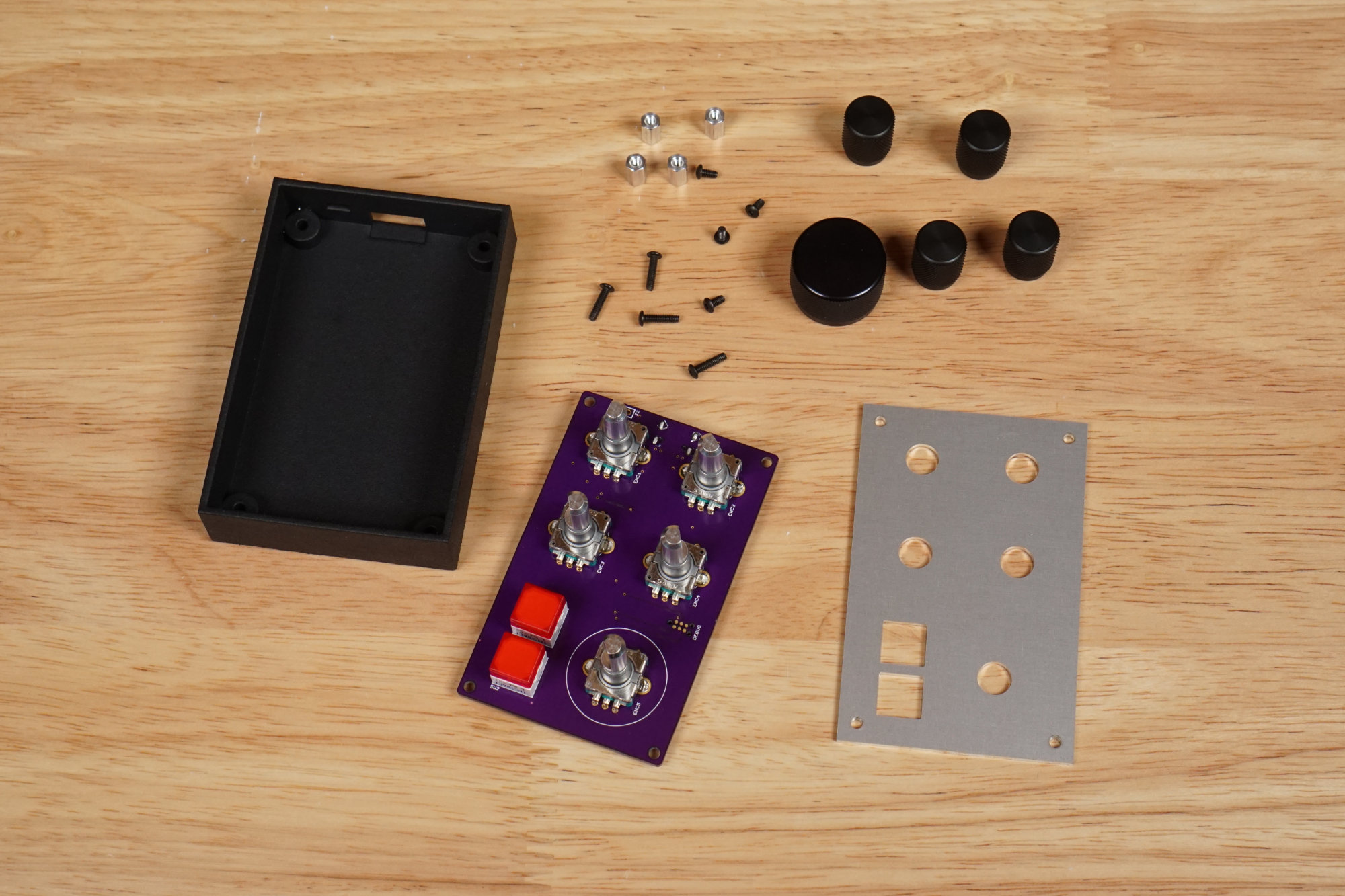
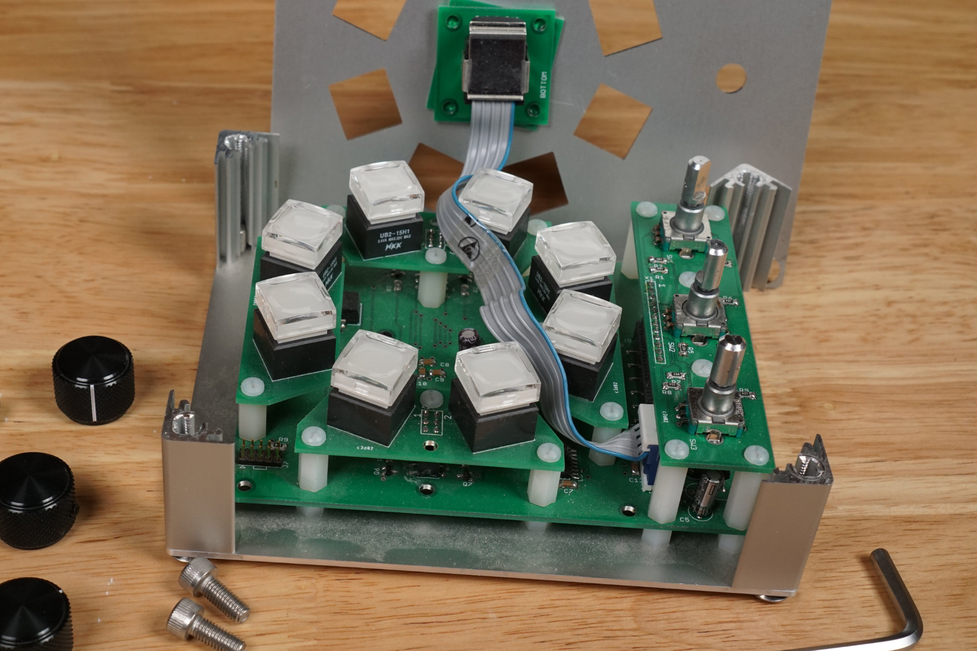
All the parts required to assemble the USB knob box.
With the hardware and software debugged, it was time to assemble the project. All the parts are shown in the above photograph.
- Attach the spacers to the rear of the top panel using the short screws.
- Lay the top panel on top of the board such that the buttons and encoder shafts extend through their corresponding holes on the panel. It will float on top of the circuit board for now. We’ll secure everything in a following step.
- Place the knobs over the encoder shafts and tighten the set screws against the flat surface of the D shaft using a 1/16″ hex screwdriver.
- Place the circuit board and panel in the enclosure starting with the end with the USB and S.BUS connectors.
- Press the panel into place in the enclosure.
- Feed the long screws through the back of enclosure, through the board, and into the bottom of spacers. Tighten with a hex screwdriver.
The final assembled USB knob box.
The photo above shows the assembled USB knob box / BMD camera remote from the top.
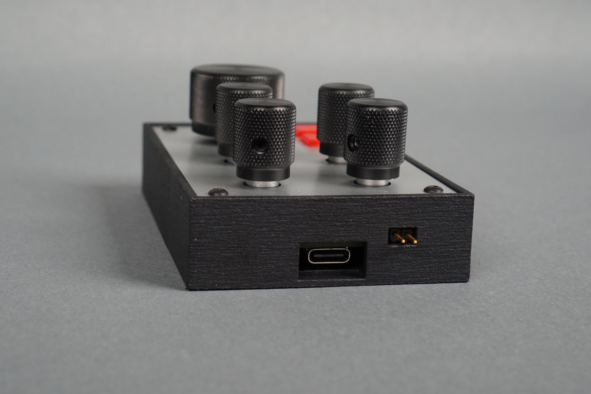
Rear view of the assembled knob box.
The photo above shows the assembled USB knob box / BMD camera remote from the rear.
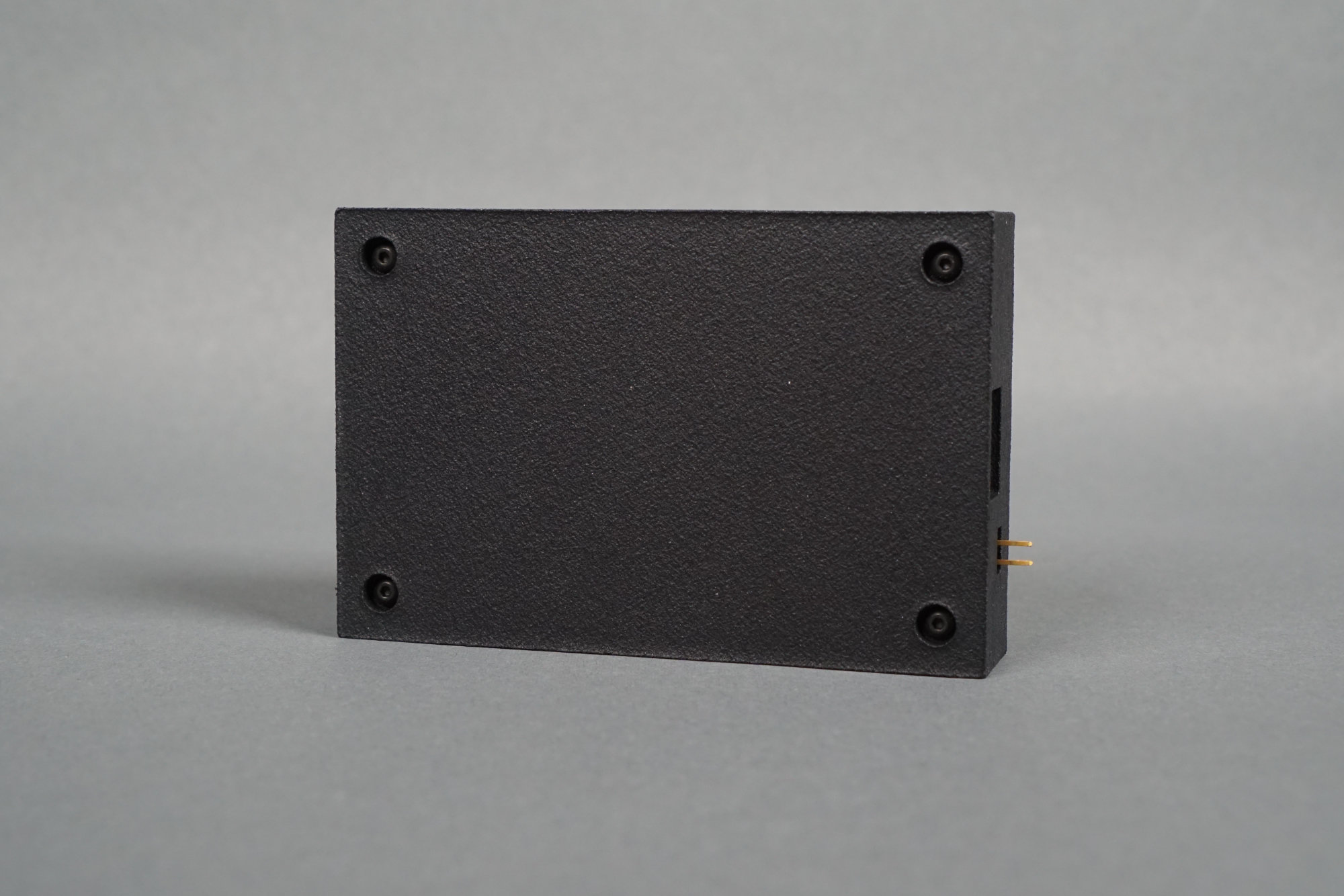
Bottom view of the USB knob box.
The photo above shows the assembled USB knob box / BMD camera remote from the bottom.
Testing with Ubuntu Linux
I didn’t do much testing with Ubuntu Linux for this project but the simplicity of lsusb and hidraw can’t be beat for initial USB hardware bringup.
Testing with Visual Studio C# .NET
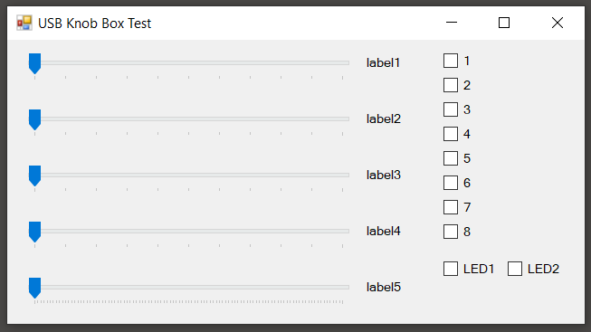
The Visual Studio C# .NET test application.
My primary testing vehicle for this project was a simple GUI application written using Visual Studio 2019 and C# .NET. The GUI is pictured in the screen capture above.
The video above shows a quick demonstration of the knob box communicating over USB with a PC running the GUI application. The video uses an earlier version of the board based on a Silicon Labs EFM8UB2 microcontroller. The functionality is identical between the newer version described in this blog post and the board shown in the video. Just a different microcontroller. That is all.
Testing with the Blackmagic Designs Micro Studio Camera 4K
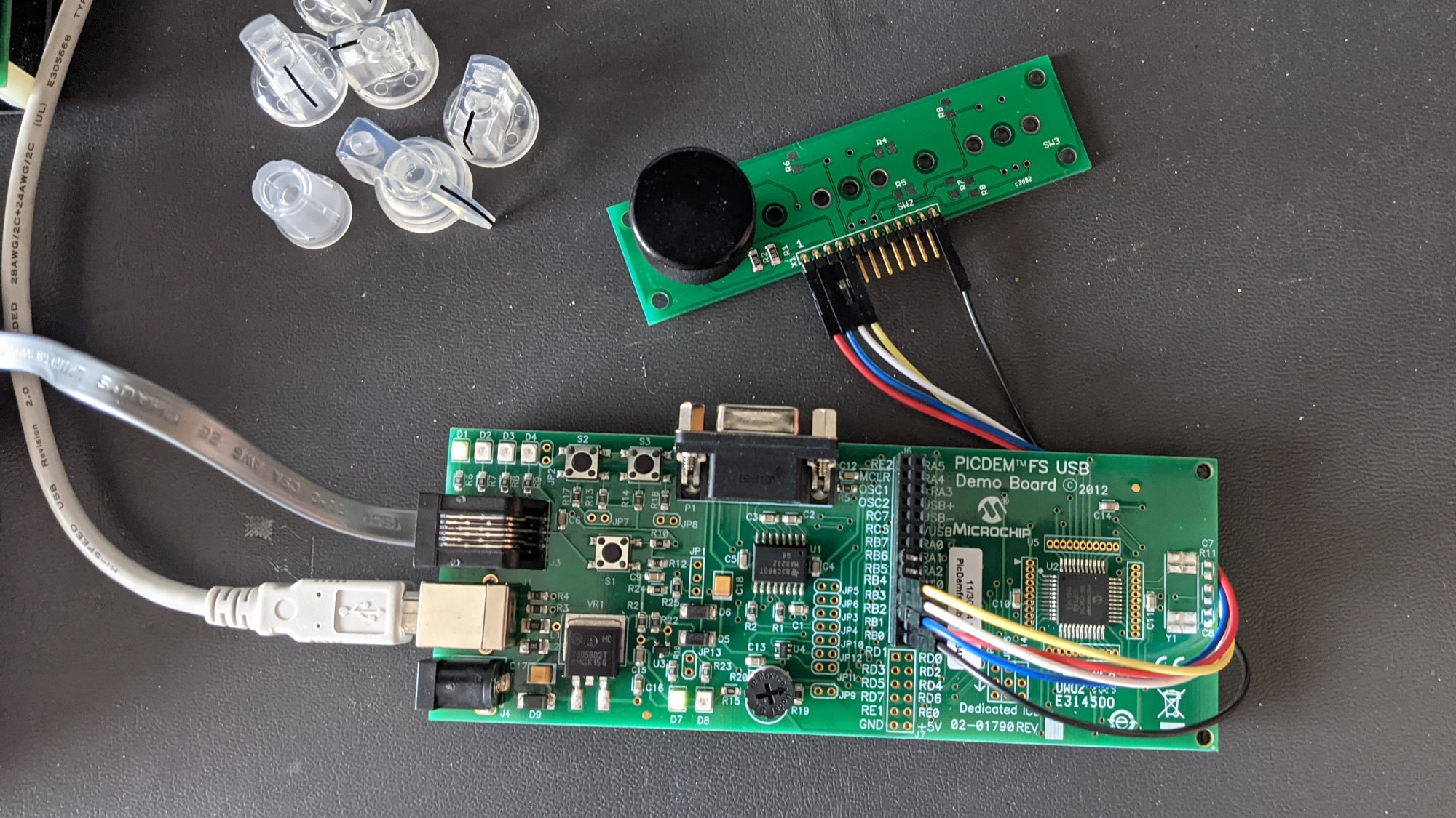
Testing the PIC18 version with the BMD Micro Studio Camera.
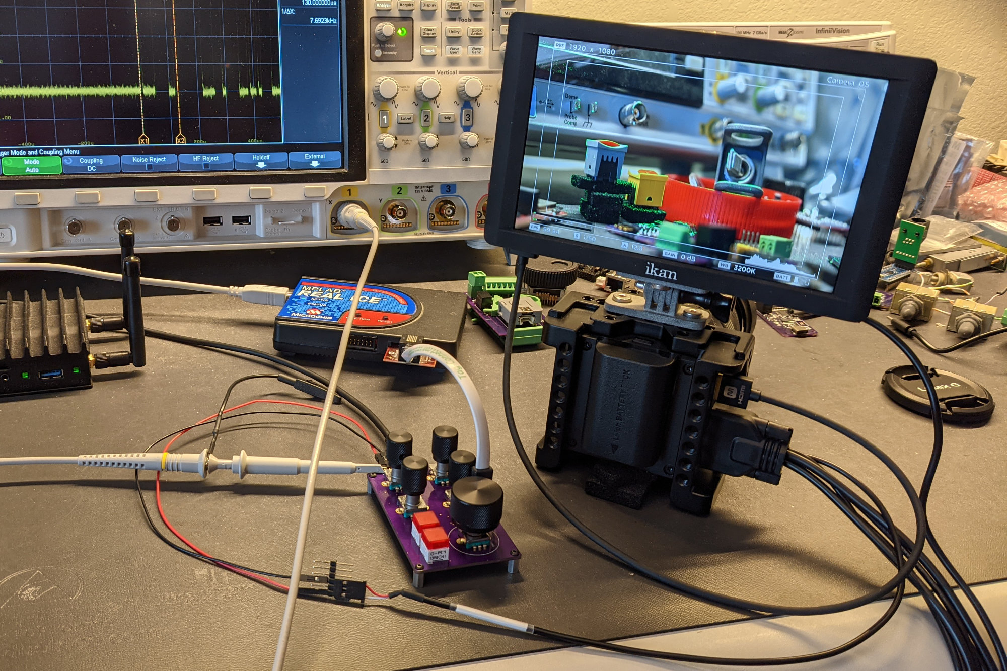
The photo above shows the setup I used while I was debugging the S.BUS control of the BMD Micro Studio Camera.
The video above shows a quick demonstration of the knob box controlling my Blackmagic Designs Micro Studio Camera 4K. The video uses an earlier version of the board based on a Silicon Labs EFM8UB2 microcontroller. The functionality is identical between the newer version described in this blog post and the board shown in the video. Just a different microcontroller. That is all.
The S.BUS output on the knob box connects to the S.BUS input on the BMD Micro Studio Camera’s hydra cable. The outside pin on the knob box is the data signal and connects to the white wire on the S.BUS input. The inside pin on the knob box is the ground and connects to the red wire on the S.BUS input. I used some short jumper wires and some long square post headers to make the connection. I’m thinking about ordering some 3 foot square post socket jumpers from EZ-Hook to make a longer cable between the two.
Final Thoughts
This was a fun project to build with a practical application. I built two versions of the project. The first version works and is based on a Silicon Labs EFM8UB2 microcontroller. Due to the chip shortage, the EFM8UB2 looks unavailable for at least the rest of the year.
The second version functions identically and is based on a Microchip PIC18F45K50 microcontroller. It’s availability at the time I wrote this was a little better than the Silicon Labs part. If you want to reproduce this project, you can use either part. Boards for both are available in Github repository for the project.
Design Files
The design files for this project are available in the project’s Github repository. All files are released under the permissive MIT open source license. If you find them useful, I always appreciate free beers. Cheers!
Todo
- SiLabs Bootloader
- PIC18 Bootloader
- Push to autofocus
- Use slots instead of holes for encoders