An animated GIF of the front panel lamps chasing each other across the panel.
After reverse engineering parts of a Grass Valley Kalypso video switcher control panel and after making a YouTube video describing how I modified a Grass Valley Series 300 transition logic panel to be a USB peripheral, it was time to reverse engineer a Grass Valley Series 300 crosspoint bus switch panel. This panel is about 20 years older than the equivalent Kalypso crosspoint bus switch panel I reverse engineered in the earlier blog post. It’s also quite a bit simpler and uses 100% off-the-shelf logic ICs with no micros or FPGAs. Read on to find out more.
The Grass Valley 300 Series Video Switcher
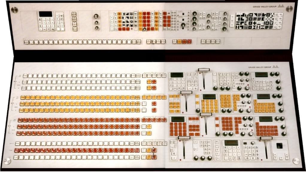
A Grass Valley Group 300 Series video switcher.
Pictured above is a Grass Valley Group 300 Series video switcher. This video switcher has three mix effects buses and a program / preview bus. The mix effects buses are color coded from top (white, #1) to middle (yellow, #2) to bottom (orange, #3). The very bottom cluster with the white and red buttons is the program / preview bus that’s used to select video signals to preview and to air. Each mix effects bus can combine a number of different video sources with different effects to create a signal that can be routed to the program / preview bus for preview and air.
The panel reverse engineered and described in this blog post is the orange M/E-3 crosspoint swtich panel on the left side of the switcher and three quarters of the way down. The crosspoint switch panel is used to select three video signals from up to 24 different video inputs to feed to the first mix effects unit. Five additional key sources and the outputs from the M/E-1 and M/E-2 units can also be selected as inputs using the buttons to the right of the main 24 columns of orange buttons. The mix effects unit then combines these selected video sources into a live, mixed video feed.
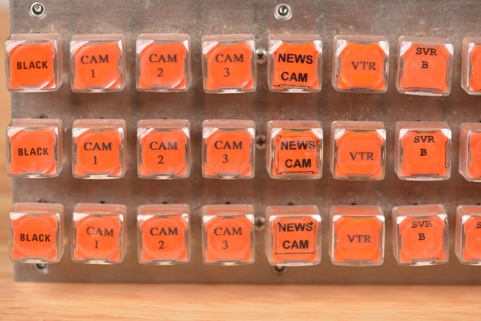
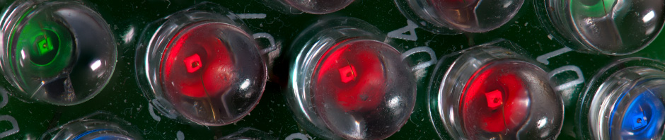
A close up of some of the crosspoint panel’s source selection buttons.
On the crosspoint switch panel, each column of switches represents a different video source. These could be, for example, studio cameras, video tape recorders, still images from still stores, text from Chyron title generators, remote truck feeds, or satellite feeds. Each row represents a different input to the mix effects unit. The top row is the key input, the middle row is the A input, and the bottom row is the B input. The photo above shows the leftmost video sources on my crosspoint switch panel.
Pressing a button in a row selects the video source in that column as an input to the mix effects unit. When a video source is selected as an input to the mix effects unit, the button at the intersection of the source column and input row is illuminated. Since there’s three rows, up to three sources can be selected as inputs to the mix-effects unit.
The buttons, knobs, and t-bar fader to the right of the crosspoint switch panel control the mix effects unit. Using these controls, the three video sources can be combined into a video feed like the one in the picture below. (I previously looked at the panel with the t-bar fader and converting it into a Halloween prop and USB peripheral in a video.)

This image consists of three input video sources: the background consisting of the anchor and set, the fire graphic above the anchor’s shoulder, and the title graphics with the anchor’s name in the foregrond.
This screen capture is from a promotional video demonstrating the mix effects capabilities of the 300 series video switcher. It is a composite of three video sources by one mix effects unit. The background with the anchor and studio set is from a camera on the A input to the M/E unit, the graphic with the fire is from a still store on the B input to the M/E unit, and the graphic with the station logo and anchor name is on the key input to the M/E unit. The M/E unit combines these three inputs into a live video feed as shown in the image.
Once the M/E unit has been configured to mix the video sources together, the bottom three rows of buttons on the switcher can be used to select the M/E output for display on a preview monitor. Just before the anchor starts talking, the technical director can cut to the M/E output and display the live composited image on air.
The Hardware
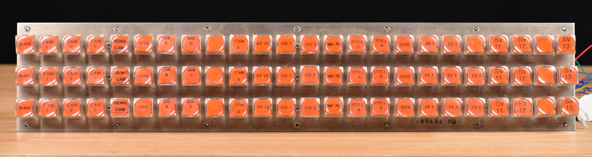
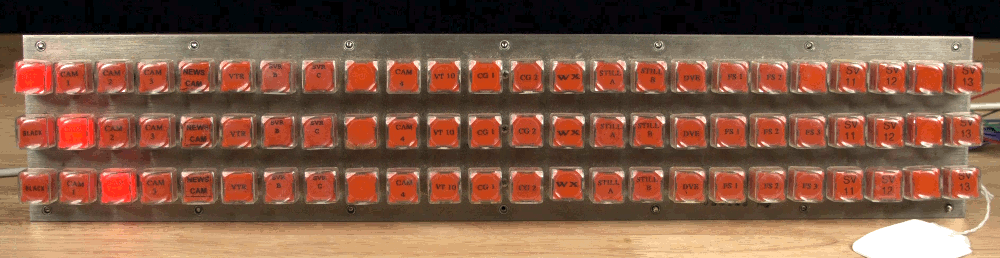
The front of the crosspoint bus switch panel. Click to embiggen.
The crosspoint switch has 72 illuminated push button switches arranged in 3 rows of 24 buttons each. The columns are spaced at a 0.9″ pitch. The rows are spaced at a 1.2″ pitch. The entire panel measures roughly 21.5″ by 4.25″.
Close up one of the switches on the crosspoint bus switch panel.
These switches are made by Electro-Mech Components. Unlike the Veetronix magnetic reed switches used on the later Grass Valley Kalypso panels, these switches use ordinary electrical contacts. The switches are held in place on the metal frame using retaining rings.
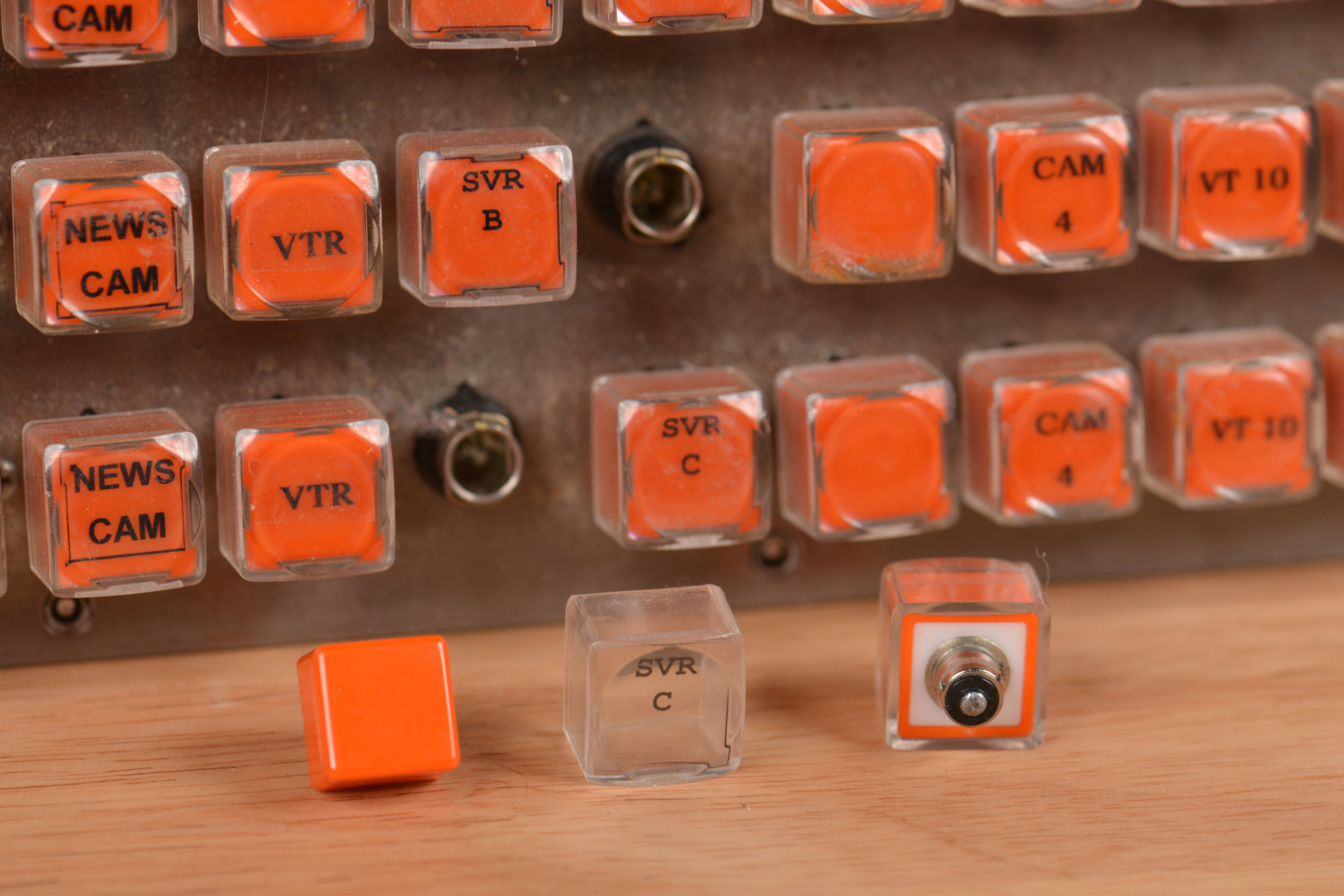
A few switches with their caps removed.
Each switch has an orange removable push button. The transparent cap can be removed from the button to insert a label indicating the video source assigned to that switch. On the rear of each button is a holder for a 12-volt midget flange base incandescent bulb.

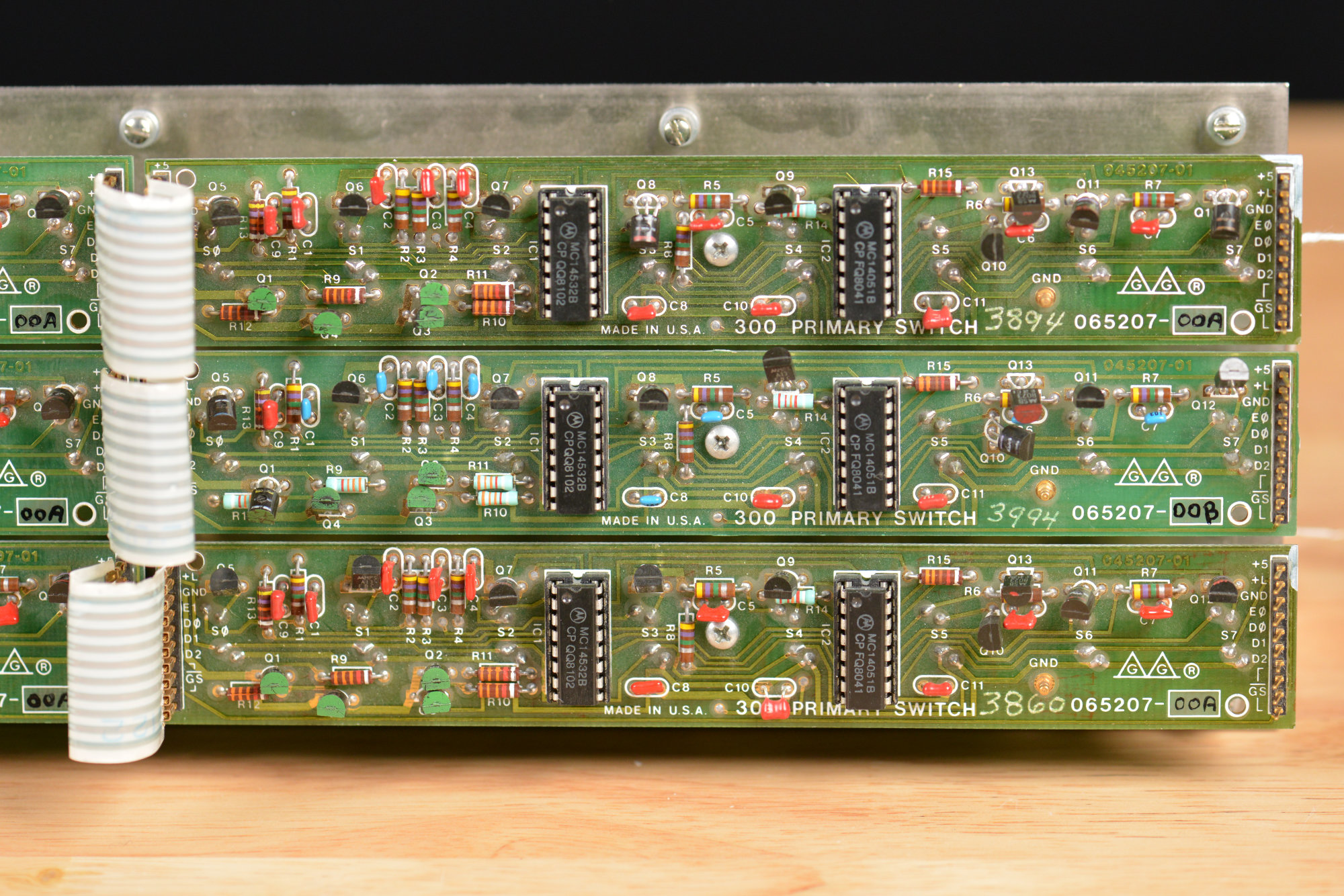
The rear of the crosspoint bus switch panel. Click to embiggen.
Looking at the back of the panel, there are nine circuit boards. Each row contains three boards and each board contains eight switches. The boards within a row are connected together using jumpers connected between pairs of 10 position headers. The rows are not connected to each other. The headers at the far left are insulated using sparsely populated header sockets. The headers at the far right are connected to the main logic board of the video switch control surface. The nine boards are identical.
Reverse Engineering One of the Boards
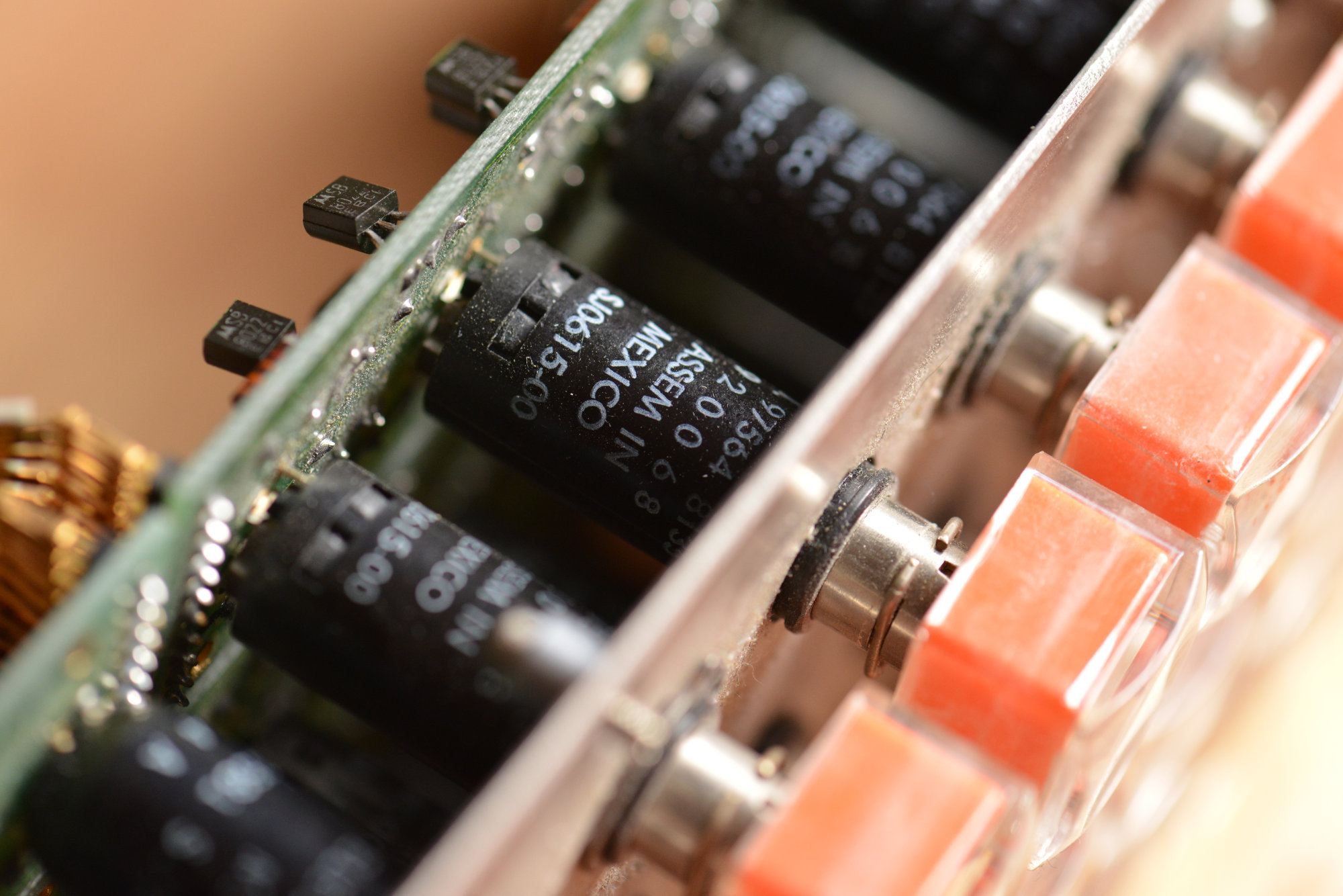
A close up of the electronics on the crosspoint bus switch panel. Click to embiggen.
The reverse engineering effort started with a quick examination of one of the nine boards, followed by the use of a digital multimeter to verify assumptions and trace connections between components.
Each board has eight switches, two headers, 13 transistors, 2 integrated circuits, and an assortment of resistors and capacitors. The eight switches are soldered to the board. Each switch has four terminals: two terminals for the lamp and two terminals for the normally open switch.
The header on the right is labeled +5, +L, GND, E0, D0, D1, D2, G0, G1, and G2. The header on the left is labeled the same except that the E0 pin is labeled E1. Using the DMM, I verified the +5 pin is the 5-volt supply, the +L pin is the supply voltage for the lamps, and the GND pin is the ground. The bulbs were type 382 midget flange base T1-3/4 incandescent lamps rated for 14 volts therefore the lamp supply voltage is 12 volts.
Since the bulb supply is 12 volts and the logic supply is 5 volts, I assumed eight of the transistors were used as low-side transistor switches to control the 12 volt lamps from 5 volt logic. Using the DMM, I was able to trace +L to a lamp pin then the other lamp pin to the collector of a transistor, the emitter of the transistor to ground, and the base of the transistor through a resistor to one of the integrated circuits. The remaining five transistors were a mystery.
Next I focused on the integrated circuits. The first integrated circuit was a MC14051B analog multiplexer/demultiplexer. The second integrated circuit was a MC14532B 8-bit priority encoder.
Functional diagram of the MC14051B analog multiplexer/demultiplexer from the second page of the datasheet.
I focused on the analog multiplexer/demultiplexer first. I used a DMM to trace out the pins. The inhibit pin connected to the G0 pin on the right header. The A, B, and C pins connected to the D0, D1, and D2 pins on both headers. The X common pin connected to +5V and the X0 to X7 outputs each connected to the base of a transistor connected to a lamp. Looks like the MC14051B is wired as a demultiplexer and controls the lamps. We’ll get in to the theory of operation in the next section.
Front page of the data sheet for the MC14532B 8-bit priority encoder.
After tracing the analog multiplexer/demultiplexer connections, I turned my attention to the 8-bit priority encoder connections. The Ein pin connected to the E1 pin on the left header. The eight D0 to D7 pins connected to the normally open terminals of the eight switches. The E1 pin is used to disable the encoder on this board if a switch is pressed on a board further to the left. Looks like the hardware can only detect one key press at a time.
The first nine connections were easy enough, but the GS, Eout, Q0, Q1, and Q2 pins connected to the base of the five mystery transistors. Further probing showed that the emitters of these five transistors were connected to ground and the collectors were connected to the G0, E0, D0, D1, and D2 pins respectively.
These transistors form a simple wired-OR bus with the rest of the boards in the row. They permit any of the boards in a row to pull the signal low without causing contention. Pullup resistors are then needed on the main controller board to keep these lines high when no board is pulling the lines low.
The final detail to note is that the G0 pin terminates on and controls this board. The G1 pin on the right header connects to the G0 pin on the left header and the G2 pin on the right header connects to the G1 pin on the left header. This makes the G0 pin enable this board, the G1 pin enable the next board to the left, and the G2 pin enable the final, leftmost board. This routing of the enable signals permits the same design to be used for all three boards in a row.

A very rough schematic of one of the eight push button boards. Reference designators are completely wrong and the resistor on the base of the transistors are missing.
After about an hour of making hypotheses, testing them with the DMM, and taking notes, I had the rough schematic shown in the image above. The schematic is missing most of the passives, the reference designators are wrong, and I do not remember which switch/lamp is where on the panel. After thinking about it some, I’m pretty sure I have the X0-X7 connections reversed on the MC14051B in the schematic. It’s not perfect, but it’s good enough to describe the logic required to turn on a lamp or determine if a button is pressed.
Turning on a Lamp
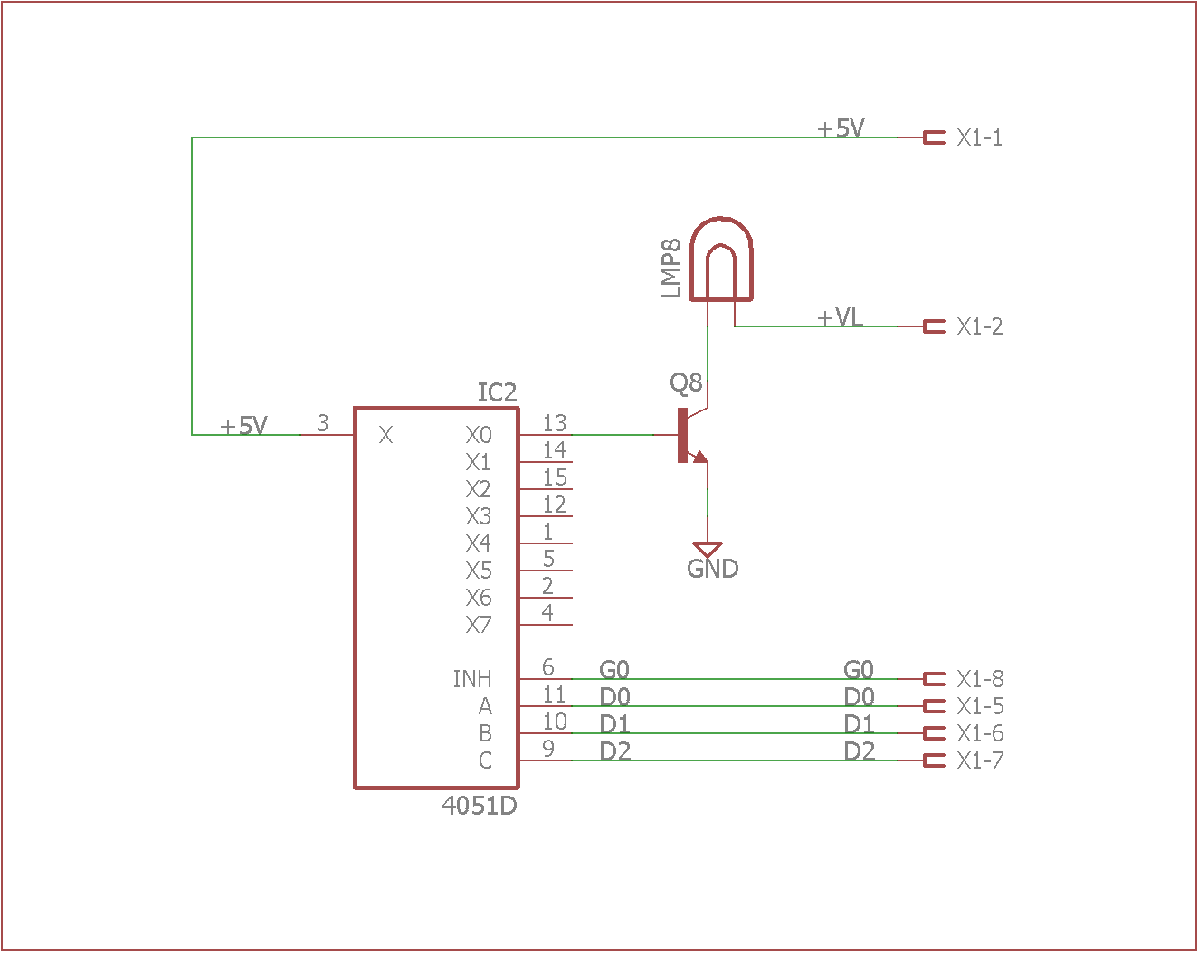
Simplified schematic for a single lamp. Setting G0, D0, D1, and D2 low will enable the demulitplixer and route five volts to the base of the transistor thus turning it on and allowing current to flow through and illuminate the lamp.
Within a row, the lamps are arranged in groups of eight according to which board they’re on. The leftmost eight lamps on the panel are enabled by the G2 pin, the middle eight lamps are enabled by the G1 pin, and the rightmost eight lamps are enabled by the G0 pin. Within a group of eight lamps on a board, the leftmost lamp is connected to X0 on the analog demultiplexer IC and the rightmost lamp is connected to X7 on the analog demultiplexer IC.
To turn on a single lamp, the system’s computer sets the Gx pin of the selected group of eight lamps low and sets the D2:D0 pins to the number of the lamp to turn on within the group of eight lamps. For example, to turn on the left most lamp (lamp 0) on the right most board (enable 0), the computer would pull G0 low while letting G1 and G2 float high and pull the three D2:D0 pins low.
This causes the INH pin on the analog demultiplixer IC to be low thus enabling the demultiplexer which routes the +5V on the X pin to the X0 pin based on the value of the D2:D0 signals. This biases the transistor and turns on the lamp. (All the signals on the headers use pullup resistors located on the system computer board to ensure lines not driven low will be pulled high.)
Detecting a Key Press
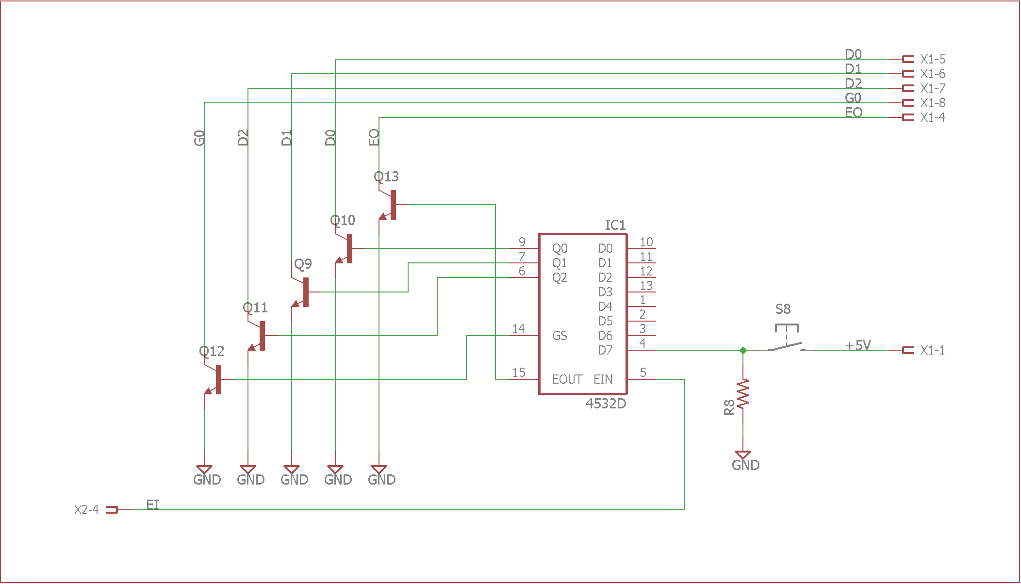
Simplified schematic for a single button. Pressing the button will pull G0 low then drive D2:D0 with the ones complement of the D2:D0 outputs of the priority encoder.
Assuming all the lamps are off, to determine that a key has been pressed, the system’s computer monitors the E0 pin. When this pin is pulled low, a key in the row has been pressed. The system computer can then read the G2:G0 signals to determine which of the three boards within a row have a pressed key and then read the D2:D0 signals to determine which key on a board has been pressed.
For example, if the left most key on the right most board is pressed, the priority encoder will drive it’s EOUT and GS outputs high and the transistors will pull the E0 and G0 lines low signifying that a key on the rightmost board has been pressed. The encoder will also drive a 7 on the Q2:Q0 outputs. This turns on all three transistors thus pulling the D2:D0 pins low indicating the leftmost key, key 0, has been pressed.
The transistors cause the Q2:Q0 outputs of the encoder to be inverted so you get the ones complement of the switch number driven on the D2:D0 lines. This is why lamp 0 is connected to the X0 pin on the analog mux IC but button 0 is connected to the D7 pin on the priority encoder IC.
Multiplexing Lamps and Key Presses
Here’s where things start to get interesting. What if a lamp is turned on and a key is pressed? In this case, the system computer and priority encoder are both pulling various combinations of the G2:G0 and D2:D0 signals low.
To determine the key that is pressed, the system computer must stop driving its ouptuts and then read the key press. While the computer is still driving its outputs, the outputs from the priority encoder and computer are OR’ed together and an odd lamp may be illuminated until system computer stops driving its outputs.
To read the key press, the control computer monitors the E0 signal. When the E0 signal goes low, the control computer stops driving its G2:G0 and D2:D0 outputs then waits for the signals not also driven by the priority encoder to be pulled high by the pullup resistors on these lines. After this delay, the control computer can read the values of the G2:G0 signals to determine the board with the pressed key and the D2:D0 signals to determine the key on the board that is pressed.
As a side effect, once the control computer is no longer driving its outputs, the lamp corresponding to that button will already be illuminated since the priority encoder is driving the enable and data signals with the levels needed for the analog demultiplexer IC to turn on that lamp.
At this point, the control computer can latch the key number, drive the signals to turn on the lamp corresponding to the key when wait for the E0 signal to go high then begin scanning the E0 signal for key presses again.
Due to the lamp and key press multiplexing schemes, this panel is really designed to only have a single lamp within a row illuminated at a time. This is consistent with the operation of the crosspoint switch in the video switcher because only 1 of the 24 sources in a row can be routed to a mix effects unit input at a time.
Controlling with a Modern Microcontroller

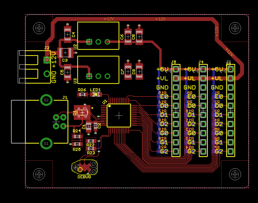
Schematic to control the panel using a modern microcontroller.
With the panel reverse engineered, it was time to try to control it using a modern microcontroller and turn it into yet another USB peripheral. The requirements for the micro were that it have twenty-one five-volt tolerant open-drain parallel GPIO pins and USB. The Silicon Labs EFM8UB2 series of parts easily fit this requirement.
The schematic above shows the completed design. It has a 12-volt power input to supply the lamps on the panel and two switching DC/DC converter regulator replacements to buck the 12-volt power input into 3.3 volts for the microcontroller and 5 volts for the analog multiplexer and priority encoders on the panel.
The microcontroller circuit is a bare bones USB design for the EFM8UB2. The GPIO pins on three of the microcontroller ports connect to the headers that connect to the Grass Valley panel. The board includes pullup resistors on each GPIO pin to keep the lines high when they’re not being pulled low by the microcontroller or the transistors connected to the priority encoders on the panel.
Board Design, Fabrication, and Assembly
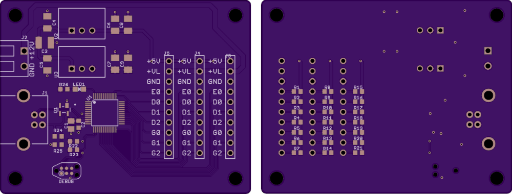
Finished board layout.
The completed board layout is shown above. The goal was to keep the USB traces as short as possible so that the impedance mismatch between the USB connector, the traces, and the microcontroller would not matter.
Board preview from the OSH Park board service.
Once the board was designed, I uploaded the gerbers to OSH Park to generate a preview and order the boards.
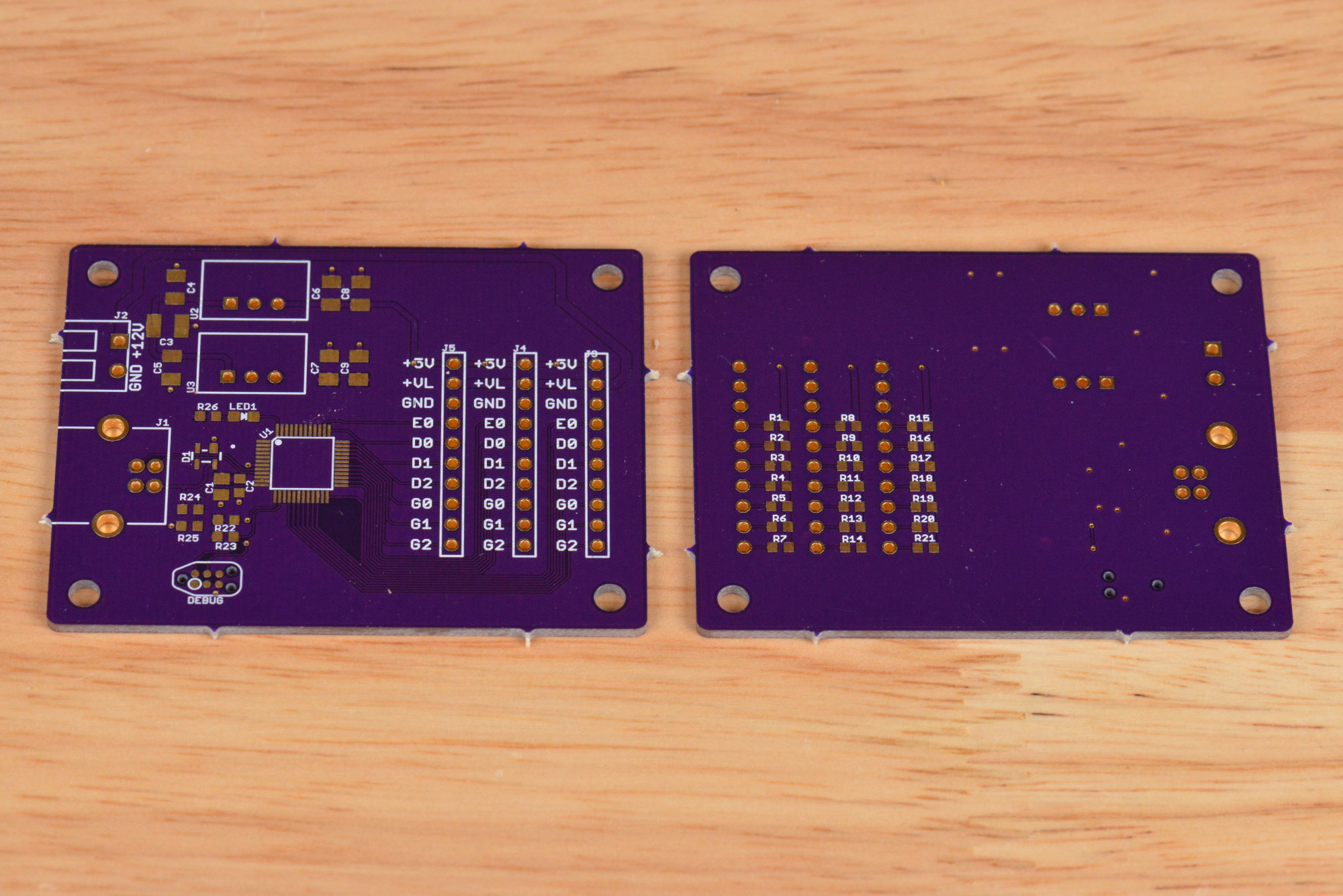
The unstuffed boards fresh back from fab at OSH Park.
The completed boards look just like the preview.
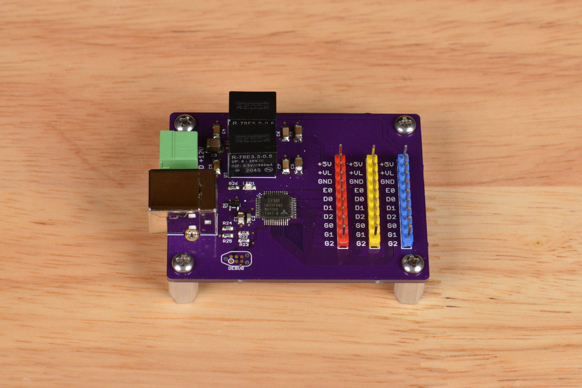
The assembled board. The red, yellow, and blue headers are a nice touch.
I procured the parts and assembled the boards. Soldering the 21 pullup resistors on the rear of the board really wasn’t that bad. The SMD resistors were definitely easier to solder than if I had used through-hole resistors.
Microcontroller Software
The software for this board was a quick rewrite of the software used for the 300 Series transition logic board project. Most of the code was left intact with only the key scanning and lamp control code modified.
This is the code to scan the buttons for presses:
for (row = 0; row < 3; row++) {
    b = GetRow (row);
    switch (state[row]) {
        case 0:
            // if key is down, turn off lamps so we can read it and go to the next state
            if ((b & 1) == 0) {
                SetLamp (row, 0xFF);
                state[row] = 1;
            }
            break;
        case 1:
            // if key is still down, read it and set that as the new key
            // when connected to usb, send the new key to host
            // if key is not still down, set the lamps back to the old value
            if ((b & 1) == 0) {
                if ((b & G0) == 0) {
                    a = 16 + ((b >> 1) & 0x7);
                } else if ((b & G1) == 0) {
                    a =  8 + ((b >> 1) & 0x7);
                } else if ((b & G2) == 0) {
                    a =  0 + ((b >> 1) & 0x7);
                }
                key[row] = a;
                SetLamp (row, key[row]);
                state[row] = 2;
                sendData[0] = row;
                sendData[1] = key[row];
                needSend = true;
            } else {
                SetLamp (row, key[row]);
                state[row] = 0;
            }
            break;
        case 2:
            // wait for key to be released
            if ((b & 1) == 1) {
                state[row] = 0;
            }
            break;
    }
}
Each row has its own state variable and the code scans each row in succession. If the E0 pin is detected low, the micro stops driving the lamps in the row, waits a cycle around the main loop, then reads the key that is pressed from the G2:G0 and D2:D0 pins. This row and key are sent to the PC over USB. The lamps are also updated locally. The state machine then waits for the E0 pin to be detected high indicating the key has been released.
The lamp code is a bit less confusing.
void SetLamp (uint8_t row, uint8_t lamp)
{
    uint8_t maskval = 0x7f; // bits we may change
    uint8_t outval = 0x71;  // all lamps off, E0 high

    if ((lamp >= 0) && (lamp <= 7)) {
        outval &= ~G2;
    } else if ((lamp >= 8) && (lamp <= 15)) {
        outval &= ~G1;
    } else if ((lamp >= 16) && (lamp <= 23)) {
        outval &= ~G0;
    }

    outval |= (lamp & 7) << 1;

    if (row == 0) {
        ROW1 = outval;
    } else if (row == 1) {
        ROW2 = outval;
    } else if (row == 2) {
        ROW3 = outval;
    }
}
The lamp code takes a row number from 0 to 2 and a lamp number from 0 to 23 and illuminates the lamp in that row. Within each row, the first 8 lamps are in group 2 on the leftmost board, the middle 8 lamps are in group 1 on the middle board, and the last 8 lamps are in group 0 on the rightmost board.
After the group is determined and the corresponding enable bit in the temporary variable is set low to enable the group, the remaining 3 bits in the lamp number are shifted into the D2:D0 bit positions in the temporary variable and the temporary variable is written to the GPIO port for that row.
Visual Studio 2019 C# .NET Application

The Windows Form GUI for monitoring and controlling the panel. It’s written in C# using the .NET framework in Visual Studio 2019 and runs on Windows 10.
The final step was to create a Windows 10 GUI to monitor key presses and control the lights. It’s very similar to the GUI I created for the analog panel meters project. Pressing a button in the GUI with the mouse colors the GUI button orange and sends a command over USB to turn on the corresponding lamp on the panel. Pressing a button on the panel, illuminates the button on the panel and sends a command to the GUI telling it to update the buttons on the screen.
Conclusion
This was a fun, quick project especially compared to the effort required to reverse engineer and control the Kalypso hardware.