
That’s a lot of hardware to rotate the synchro receiver on the right!
In the last project, I built a synchro-to-digital converter to display a synchro’s shaft angle on a small OLED display. In this project, I reverse the process and build a digital-to-synchro converter that sets a synchro’s shaft to the angle entered into a terminal window.
Synchro Torque Chains
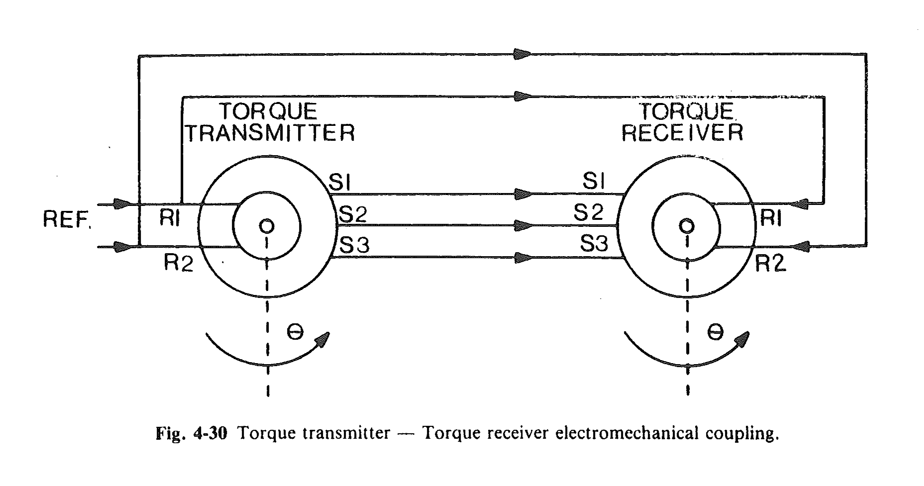
Figure 4-30. Torque transmitter – torque receiver electromechanical coupling from Chapter four of the Analog Devices Synchro and Resolver Conversion Handbook.
In my first synchro post, I covered the basics of a synchro transmitter. To the synchro transmitter, we’re going to add a synchro receiver that’s connected to form a torque chain. In a torque chain, the rotors of both synchros are connected to the same reference voltage and the stator wires are connected between the two synchros. This is depicted schematically in the figure above from the Analog Devices Synchro and Resolver Conversion Handbook.
When two synchros are connected in a torque chain, turning the shaft of the transmitter to an angle causes the shaft of the receiver to turn to the same angle. If the load on the torque receiver is low, for example a needle on an indicator, the torque receiver can be used to directly move the attached load to the same angle set by the transmitter. This was often done on aircraft automatic direction finder (ADF) equipment to rotate the needle on the ADF indicator in the cockpit to the ADF receiver’s antenna’s null angle.
If the load to be moved is too great for the synchro receiver to move on its own, the receiver can be replaced with a control transformer and incorporated into a servo loop. An example of this application would be using a gunsite to control the aim of a remote gun turret on a fighter plane.
The goal in this project is to replace the synchro transmitter on the left side of the torque chain schematic with modern electronic components so that an angle may be typed into a terminal window connected to a microcontroller and the synchro receiver’s shaft turns to that angle.
Commercial Digital-to-Synchro Converters
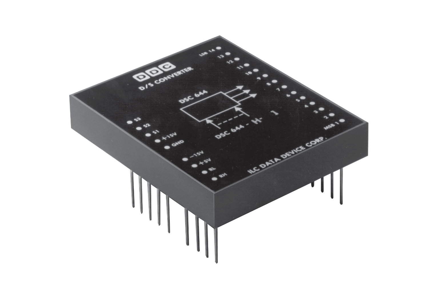
Data Device Corporation DSC-644 digital-to-synchro converter. The module measures 7.94 x 6.67 x 1.32 cm and weighs 145 g.
Commercial digital-to-synchro converters do exist but they’re “click here for a quote” expensive and basically unobtanium to hobbyists. One such commercial converter is pictured above. It takes in a 14-bit angle value on the pins on the right and the reference voltage on the RL and RH pins then outputs the synchro format voltages corresponding to the given angle on the S1, S2, and S3 pins. Since this is a 14-bit converter, it has a precision of approximately 1.32 arc minute. The accuracy is a bit less at ±4 arc minutes.
A converter like this might be used in a flight simulator. In a flight simulator, it would take an output of the simulator’s modeling engine, e.g. the aircraft altitude, and convert it into an analog synchro format signal that could drive the exact same altitude indicator used in the real aircraft.
Literature Review
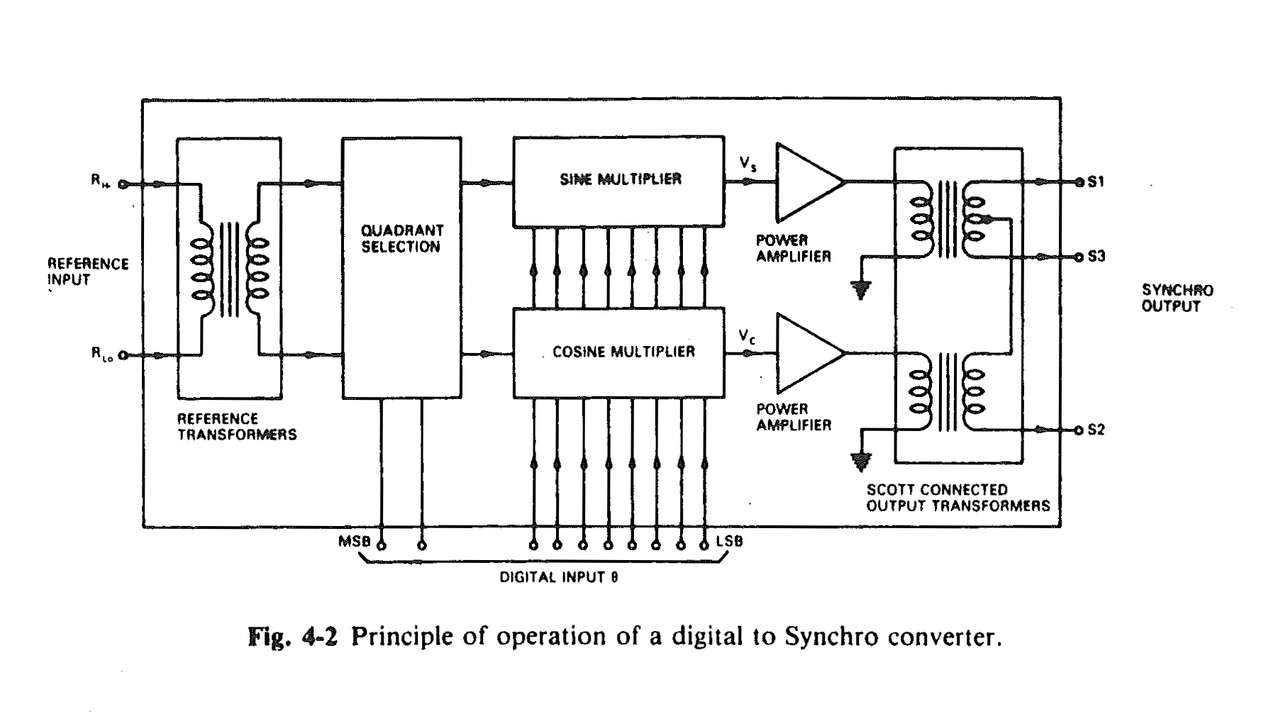
Figure 4-2. Principle of operation of a digital-to-synchro converter from Chapter four of the Analog Devices Synchro and Resolver Conversion Handbook.
With a commercial converter out of the realm of possibility, it was time to look for an alternate solution. Fortunately, Chapter four of the Analog Devices Synchro and Resolver Conversion Handbook has a great explanation of how a digital-to-synchro converter works. Figure 4-2 above is a block diagram of such a converter from the handbook.
The digital-to-synchro converter takes in the reference voltage and multiplies it by the sine and cosine of the desired shaft angle to form a resolver format voltage. The resolver format voltages are fed to a Scott-connected output transformer that converts the resolver format voltages into synchro format voltages. (A Scott-connected transformer transforms two input AC voltages 90° apart into three AC voltage outputs that are 120° apart. Scott-connected transformers are covered in chapter two of the handbook.)
Perfect! An input transformer, two multiplying DACs, two power amps, and a Scott-connected transformer! Project done. Except guess what? Small Scott-connected transformers are impossible to find too.
I’m still not giving up. Maybe there’s a way to drive the three stator signals directly without needing the Scott-connected transformer.
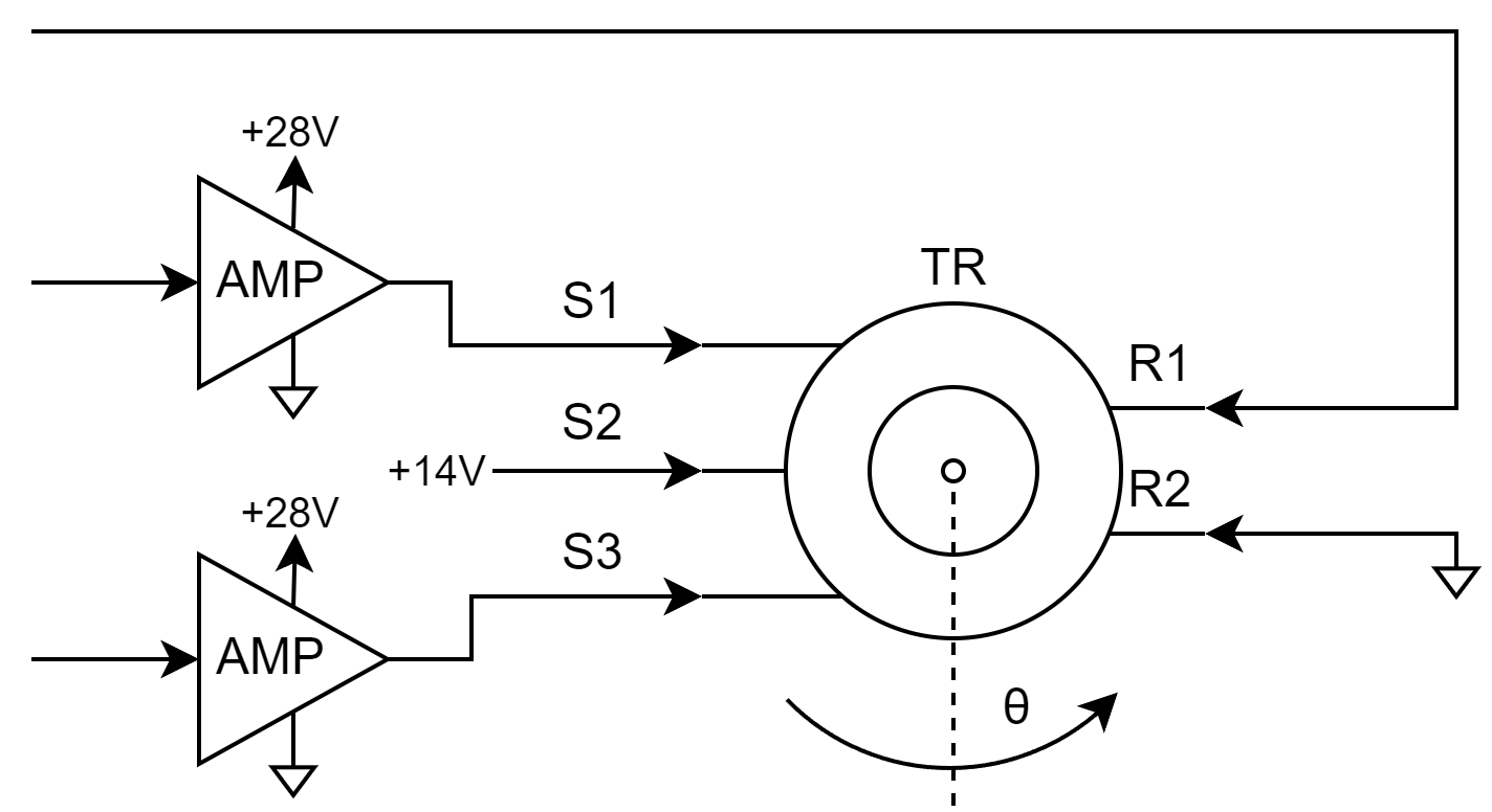
schematic
While looking at schematics for some aircraft instruments, I noticed one that used a single +28 VDC supply. In this instrument, the S2 terminal on the synchro was connected to a +14 VDC regulator while the S1 and S3 terminals were connected to amplifiers as shown in the figure above. If this worked with a terminal connected to the midpoint of the unipolar power supply, could this work with the S2 terminal connected to the ground (aka midpoint) of a bipolar power supply?
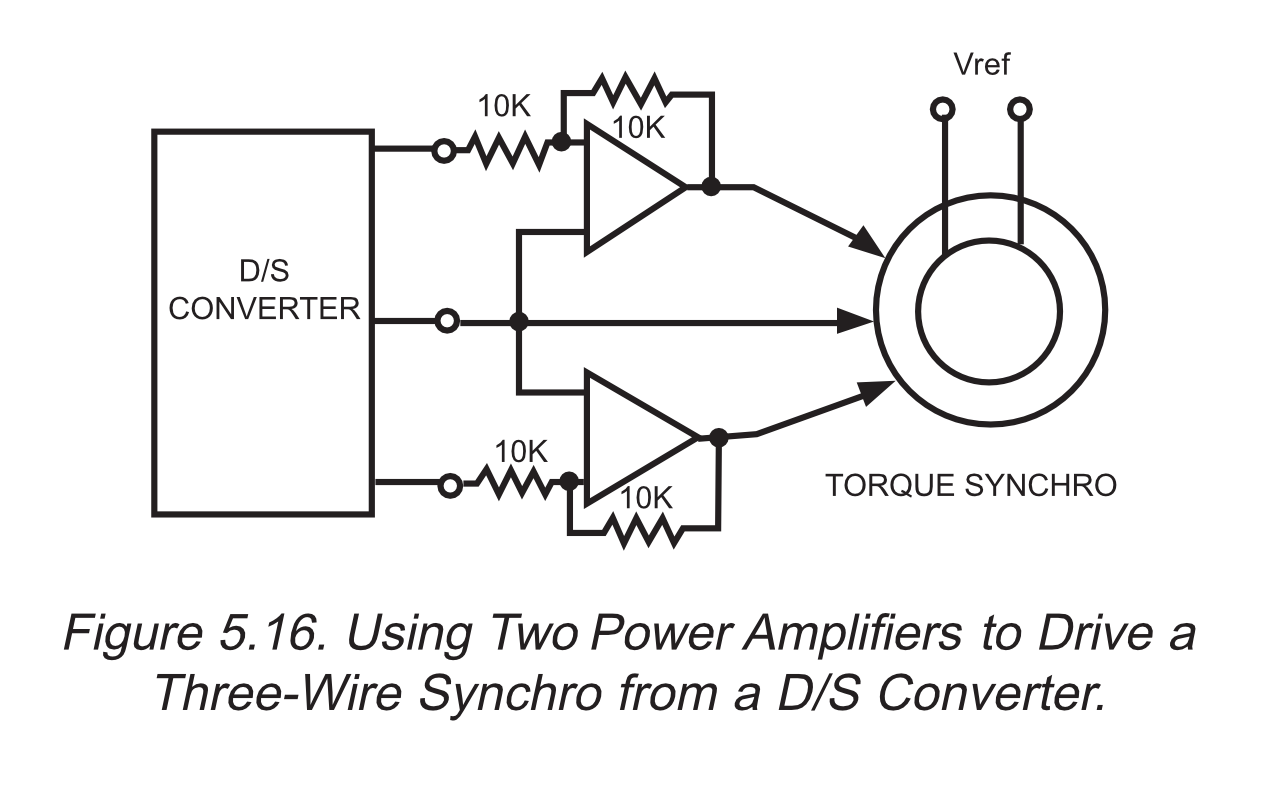
Figure 5-16 from the Data Device Corporation Synchro/Resolver Conversion Handbook. PDF link in references section at the end of this post.
After doing a bit more research, I found the Data Device Corporation Synchro/Resolver Conversion Handbook. Figure 5-16 (reproduced above) and the accompanying text in the handbook confirmed that this was possible albeit for a slightly different application:
“Figure 5.16 shows how two external power amplifiers may be used to drive one or more three-wire synchro receivers in parallel (or a high-power torque synchro). This is possible because of the Y-connection configuration of the synchro receiver stator windings. It can be shown that supplying the high-level energy to two of the three input lines, and directly connecting the third (ground is the common connection) is just as effective as using three power boosters.”
We found a way. Now let’s build it!
The Plan
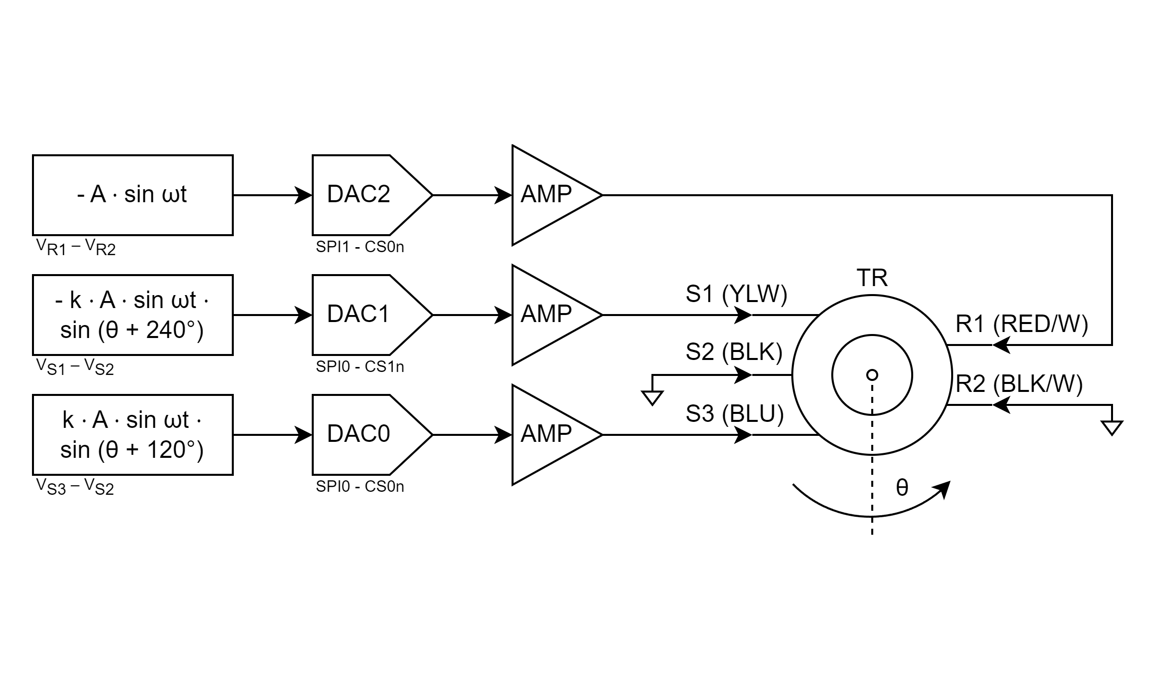
The completed plan.
The plan is to create the reference and synchro format voltage waveforms in software, use DACs to convert these to analog signals, amplify the signals using power amplifiers, and then connect the amplifer outputs directly to the synchro receiver as shown in the figure above. Note that the S2 and R2 terminals of the synchro receiver are connected directly to ground and the amplifiers will require a bipolar power supply. Since this system has no output transformer, this converter will lack the galvanic isolation of the commercial converters.
Recall from the prior synchro-related post that the equation for the synchro’s reference voltage is:
Vref = VR2 – VR1 = A ⋅ sin ωt
And the equations for the synchro-format voltages are:
VS1 – VS3 = k ⋅ A ⋅ sin ωt ⋅ sin θ
VS3 – VS2 = k ⋅ A ⋅ sin ωt ⋅ sin (θ + 120°)
VS2 – VS1 = k ⋅ A ⋅ sin ωt ⋅ sin (θ + 240°)
Referring to the block diagram above, DAC2 and its associated power amplifier are connected from R1 to R2 so we need to generate the negative of VR2 – VR1:
VR1 – VR2 = – A ⋅ sin ωt
Then S2 is connected to ground so the synchro format equations become:
VS1 – VS3 = k ⋅ A ⋅ sin ωt ⋅ sin θ (eq. i)
VS3 – 0 = k ⋅ A ⋅ sin ωt ⋅ sin (θ + 120°) (eq. ii)
0 – VS1 = k ⋅ A ⋅ sin ωt ⋅ sin (θ + 240°) (eq. iii)
DAC1 and its associated power amplifier are connected from S1 to S2 (ground) so we need to generate the negative of eq. iii:
VS1 = – k ⋅ A ⋅ sin ωt ⋅ sin (θ + 240°)
DAC0 and its associated power amplifier are connected from S3 to S2 (ground) so we need to generate eq. ii as is:
VS3 = k ⋅ A ⋅ sin ωt ⋅ sin (θ + 120°)
Finally, it can be shown that the relationship between VS1 and VS3 shown in eq. i is maintained using these connections. The coupling transformation ratio, k, will be implemented in the amplifier gains rather than in software.
Building a Power Arbitrary Waveform Generator
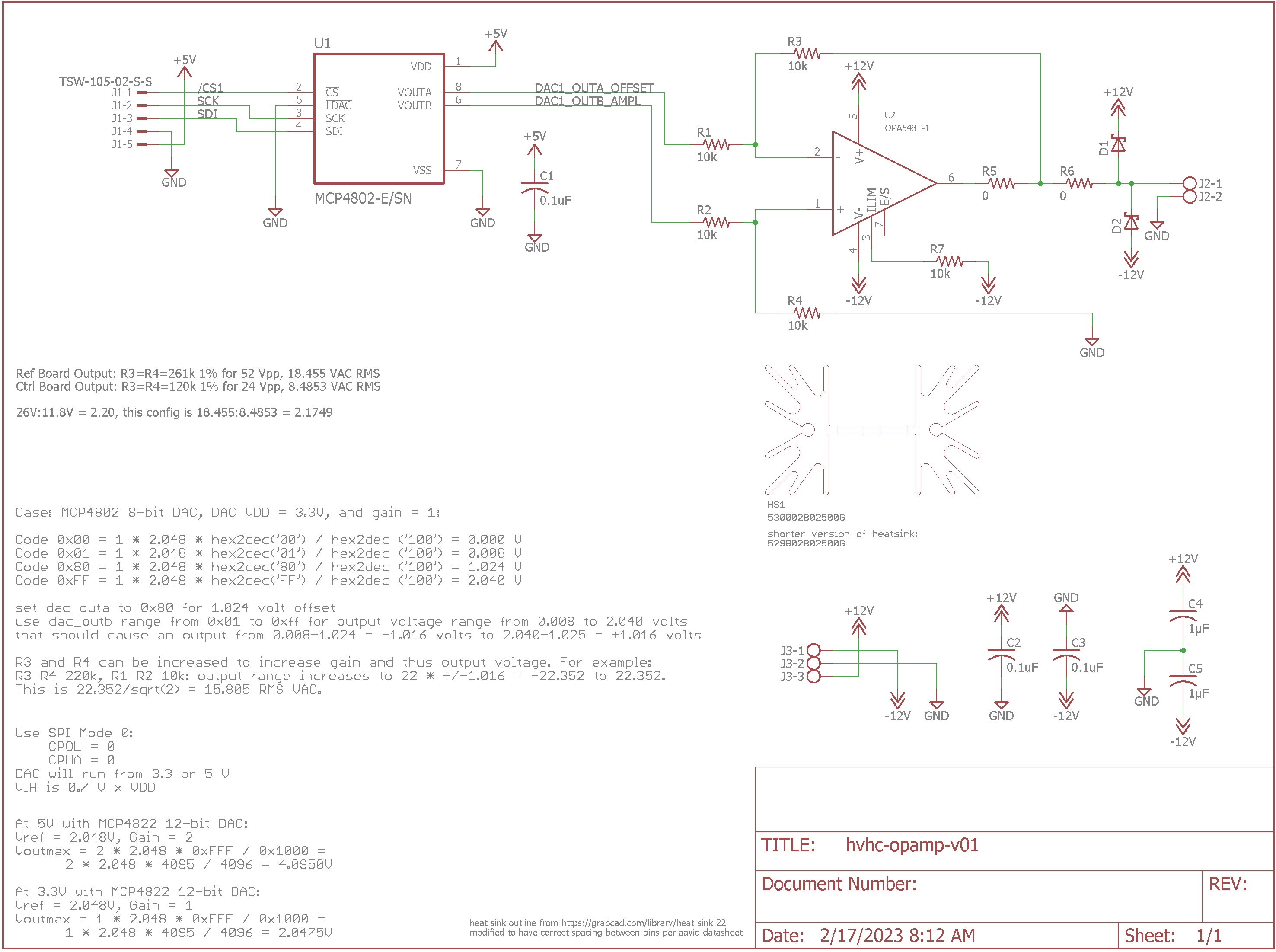
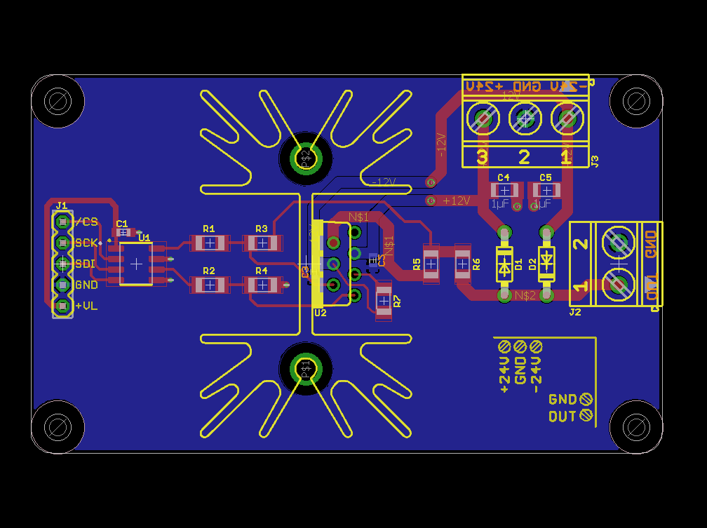
Power AWG schematic.
For this project, I decided to use the Texas Instrument OPA548 high-voltage, high-current op amp. It’s rated for a 30 V bipolar power supply and can supply 3 A continuous / 5 A peak. Compared to the LT1010-based circuit used in the synchro-to-digital project, the OPA548 circuit will allow my synchro to run much closer to its rated 26 VAC rotor voltage and is capable of supplying 20 times as much current.
The schematic for the circuit is shown above. The theory of operation is the same as for the LT1010-based circuit. A DAC supplies an offset voltage on channel A and a 400 Hz sine wave on channel B. These two voltages are fed to the power op amp which is configured to multiply the two voltages by R3/R1 and R4/R2 respectively and subtract the offset voltage from the sine wave. DAC channel A is set to 1/2 of its reference voltage or 1.024 volts while DAC channel B is used to generate a sine wave ranging from 0.008 to 2.040 volts.
This results in a sine wave centered at ground with a positive peak voltage of
2.040 ⋅ R4/R2 – 1.024 ⋅ R3/R1
and a negative peak voltage of
0.008 ⋅ R4/R2 – 1.024 ⋅ R3/R1
With R3 = R4 = 261 kΩ and R1 = R2 = 10.0 kΩ, this results in a positive peak voltage of
261 kΩ / 10 kΩ – 2.040 V – 261 kΩ / 10 kΩ ⋅ 1.024 V = 26.518 V
and a negative peak voltage of
261 kΩ / 10 kΩ – 0.008 V – 261 kΩ / 10 kΩ ⋅ 1.024 V = -26.518 V
This is an AC RMS voltage of 18.751 V which is still a bit lower than the synchro’s rated rotor voltage of 26 VAC. We’ll demonstrate that it is sufficient to move the synchro in the next section of this post.
Power AWG board layout.
The board layout is shown above. The DAC’s SPI input is on the left side of the board, power supply connections are on the top of the board, and the output is on the right side of the board. The power supply is decoupled using 1 µF caps across each of its rails at the input connector and 0.1 µF caps on the bottom of the board as close as possible to the power supply terminals of the op amp. Since the synchro is an inductive load, flyback protection diodes were added between the output and each power supply rail.
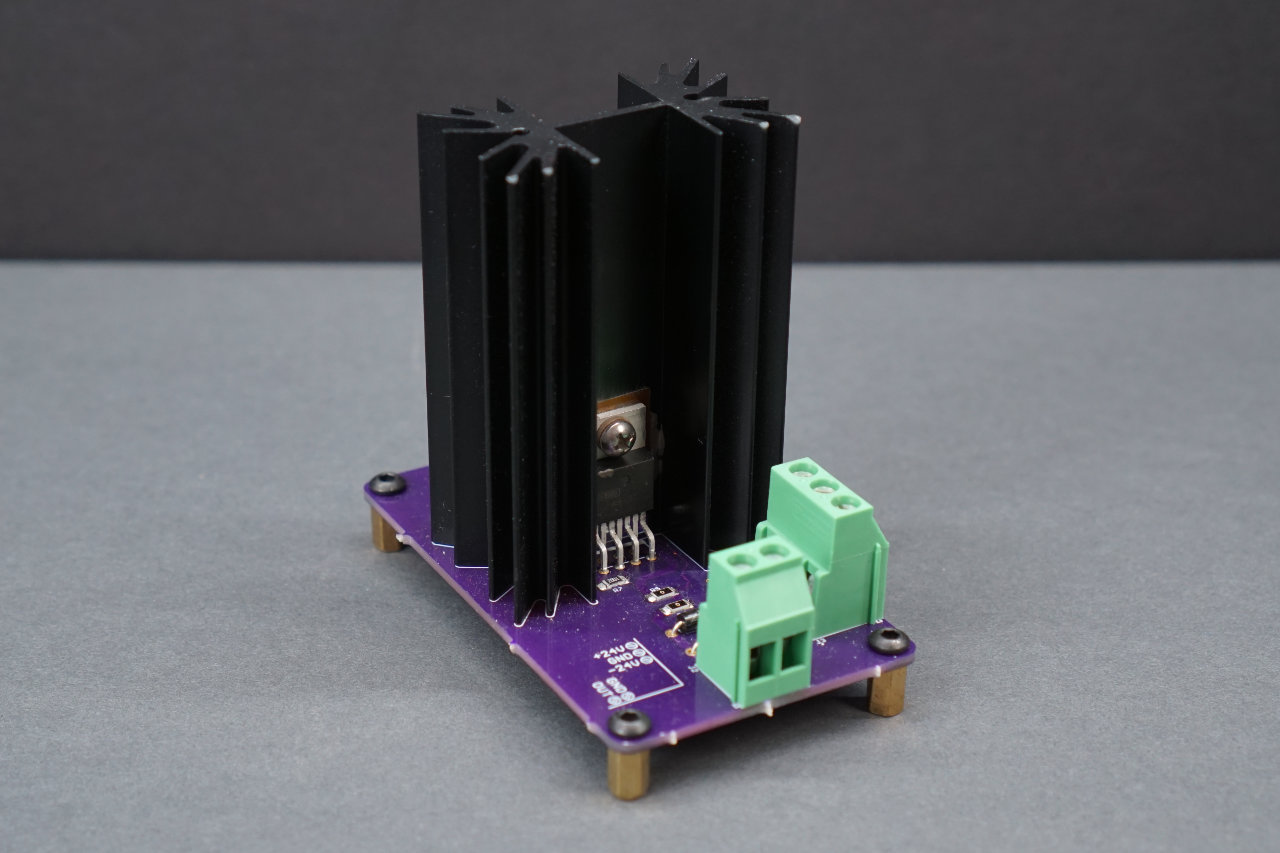
The completed power arbitrary waveform generator.
The completed board is shown above. Since this board has a skyscraper of a heat sink and I have no idea if / when it will go up in flames, I decided to nickname it the towering inferno.
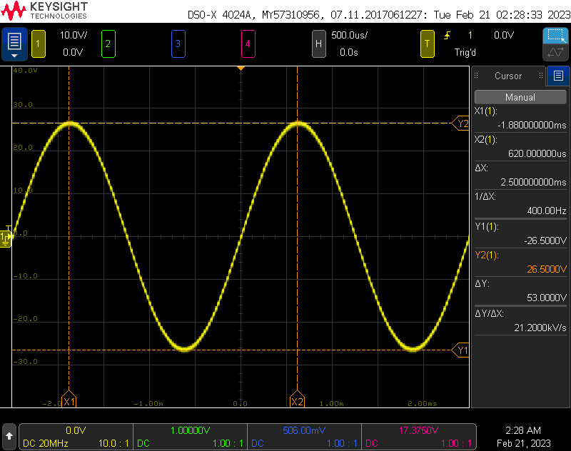
Initial testing with a bench supply and oscilloscope showed the board produced the expected 53 VPP 400 Hz AC waveform as shown in the oscilloscope screen capture above.
Will They Blend Track?
Since my synchro receiver is rated for operation at 26 VAC and I’m only generating a voltage of 18.751 VAC, I decided to connect a synchro transmitter and a synchro receiver together in a torque chain to ensure the synchros would work at the lower reference voltage. Turning the transmitter shaft resulted in the receiver shaft tracking the transmitter shaft’s motion. This is demonstrated in the video above. Since the synchro receiver was capable of working at the lower reference voltage, I decided to move forward with the project.
Building More Power AWG Channels
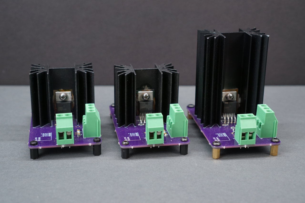
I built a total of three of these boards. Two shorter ones for the synchro format voltages and one taller one for the reference voltage.
I built up two more power AWG boards. These boards need to incorporate the coupling transformation ratio, k, of the synchro receiver into the op amps’ gains. For my synchros, this is the ratio of the stator winding voltage to the rotor winding voltage or 11.8 V / 26 V = 0.4538.
Since the reference voltage board had a gain of 26.1, these boards would need a gain of k ⋅ 26.1 = 11.8 / 26 * 26.1 = 11.845. I went with a gain of 12. This makes R3 = R4 = 120 kΩ and R1 = R2 = 10 kΩ on these boards. With these resistors, the sine wave output will range from -12.192 V to +12.192 V. This is 8.621 VAC. Finally as a check:
k from the synchro’s specs: 11.8 V / 26 V = 0.4538
k with my boards’ output voltages: 8.621 V / 18.751 V = 0.4671
Even if my voltages are a bit low, they’re in the correct ratio to each other. I also found a shorter version of the heat sink with the same footprint and used that heat sink on these boards.
Putting it Together

schematic
This project was already going to have a ton of wires. To increase the reliability of the project, I built a quick board to split off the SPI buses from the Raspberry Pi Pico that would be used to control everything. The schematic is shown above.
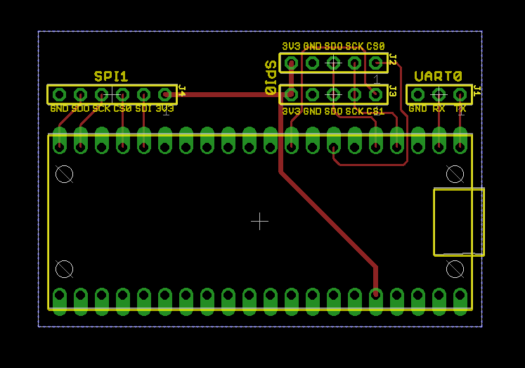
board
The completed board layout is shown above.
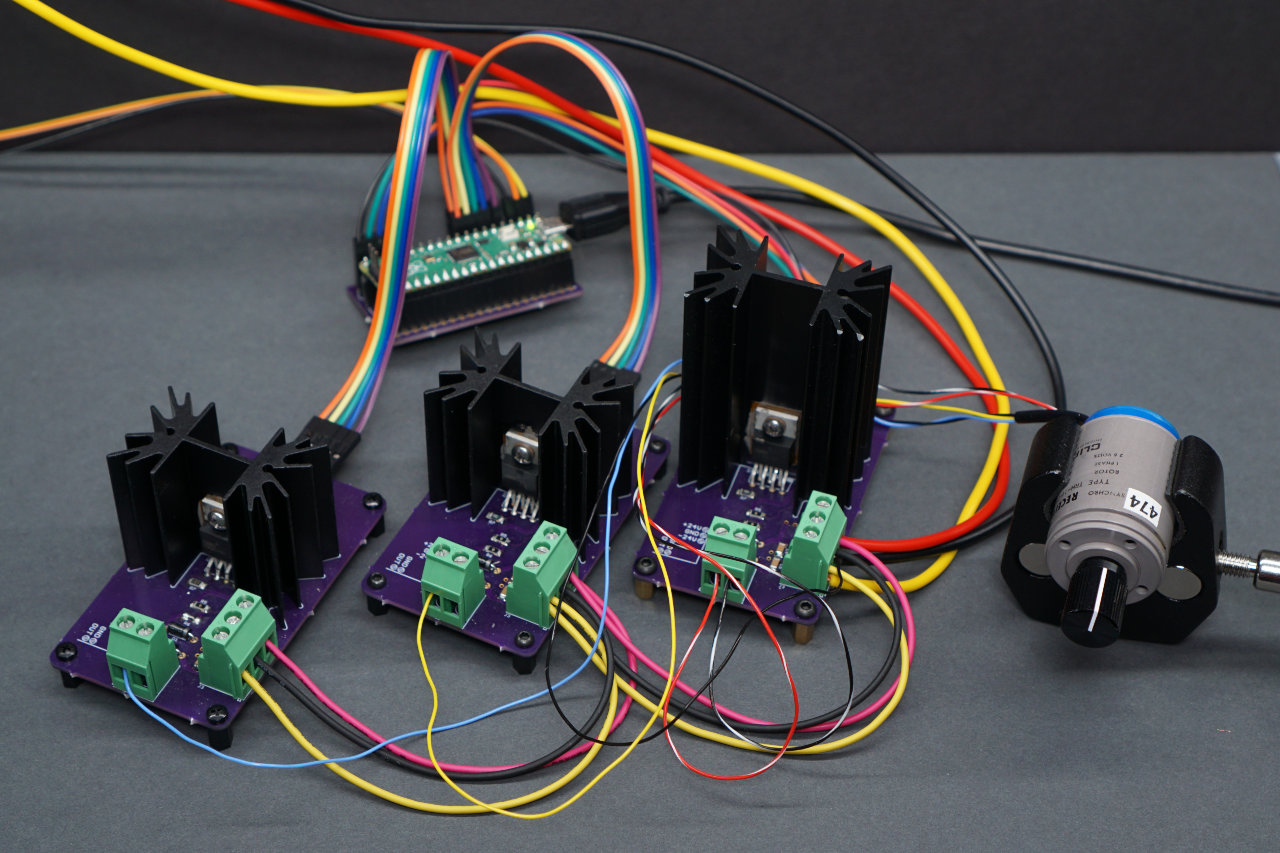
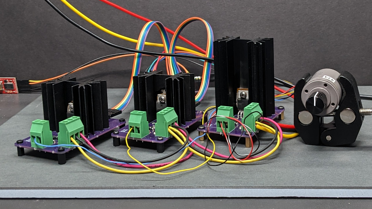
All the boards connected and powered up. Left to right are DAC0, DAC1, and DAC2 then the synchro receiver. In the back is the Rapsberry Pi Pico development board.
The photo above shows the three power AWG boards and the Pico dev board connected together. The SPI chip selects and synchro are connected as shown in the block diagram in the “The Plan” section of this post.
Software
I don’t want to get too deep into the software except to point out the functions of few small sections of the code. The complete software can be downloaded using the links at the end of this post.
This is the storage for the sine wave:
// sine lookup table
// a=sin((0:99)*2*pi/100);
// b=round(a*127);
// min(b) ans = -127
// max(b) ans =  127
// b(1)   ans =  0
static const int8_t sine[100] = {
     0,    8,   16,   24,   32,   39,   47,   54,   61,   68,
    75,   81,   87,   93,   98,  103,  107,  111,  115,  118,
   121,  123,  125,  126,  127,  127,  127,  126,  125,  123,
   121,  118,  115,  111,  107,  103,   98,   93,   87,   81,
    75,   68,   61,   54,   47,   39,   32,   24,   16,    8,
     0,   -8,  -16,  -24,  -32,  -39,  -47,  -54,  -61,  -68,
   -75,  -81,  -87,  -93,  -98, -103, -107, -111, -115, -118,
  -121, -123, -125, -126, -127, -127, -127, -126, -125, -123,
  -121, -118, -115, -111, -107, -103,  -98,  -93,  -87,  -81,
   -75,  -68,  -61,  -54,  -47,  -39,  -32,  -24,  -16,   -8
};
It is 100 samples long and the values run from -127 to +127. The sine wave is scaled and offset and played out each of the three DACs at a sample rate of 40 kHz resulting in three 400 Hz signals.
This code initializes both channels of all three DACs to their mid scale value of 0x80:
    // initialize dacs on spi 0
    dacWrite16 (spi0, SPI0_CS0n_PIN, 0x3800); // write 0x800 to DAC 0 A
    dacWrite16 (spi0, SPI0_CS0n_PIN, 0xB000); // write 0x000 to DAC 0 B
    dacWrite16 (spi0, SPI0_CS1n_PIN, 0x3800); // write 0x800 to DAC 1 A
    dacWrite16 (spi0, SPI0_CS1n_PIN, 0xB000); // write 0x000 to DAC 1 B
    dac0B = 0;
    dac1B = 0;

    // initialize dacs on spi 1
    dacWrite16 (spi1, SPI1_CS0n_PIN, 0x3800); // write 0x800 to DAC 2 A
    dacWrite16 (spi1, SPI1_CS0n_PIN, 0xB000); // write 0x000 to DAC 2 B
    dac2B = 0;
Once this code is done executing, channel A will not be changed again leaving it at its mid scale value and creating the offset voltage fed into the (-) terminal of the op amps.
When an angle is entered into the terminal window followed by a press of the return key, this code is executed:
    target = fmod (atof (buffptr), 360.0);
    newScale0 =  sin ((target + 120)*M_PI/180.0); // s3 / blue
    newScale1 = -sin ((target + 240)*M_PI/180.0); // s1 / yellow
    printf ("               YL-BU  BU-BK   BK-YL\n");
    printf ("target: %6.0f %6.2f %6.2f %6.2f\n",
        target,                // target angle
        newScale1 - newScale0, // target s1-s3
        newScale0 - 0,         // target s3-s2
        0 - newScale1);        // target s2-s1
The code ensures the entered angle is between 0° and 360° and writes it to the target angle variable. The rest of the code is for debugging purpose and the values of newScale0 and newScale1 are thrown out.
This code executes 100 times a second using a repeating timer:
    // gradual move
    float diff = fmod ((target - theta + 180), 360) - 180;
    diff = diff < -180 ? diff + 360 : diff;
    if (fabs(diff) == 180) { // always move CW for 180 degree difference
        theta++;
    } else if (diff < 0) {   // move CCW
        theta--;
    } else if (diff > 0) {   // move CW
        theta++;
    } else {                 // no move needed
        // nothing
    }

    // move to theta
    newScale0 =  sin ((theta + 120)*M_PI/180.0); // s3 / blue
    newScale1 = -sin ((theta + 240)*M_PI/180.0); // s1 / yellow
    critical_section_enter_blocking (&scale_critsec);
    scaleDac0 = newScale0;
    scaleDac1 = newScale1;
    critical_section_exit (&scale_critsec);
This code determines the difference between the target angle in target and the actual angle in theta then steps theta in the shortest direction to the target angle. Differences of 180° always go clockwise. Gradual moves result in less instantaneous current draw than sudden moves. Once the new value of theta is calculated, the new scaling factors for DAC0 and DAC1 are calculated and written to newScale0 and newScale1.
With new values calculated, they’re transferred to the variables used by the 40 kHz repeating timer running on core 1 where they’re used to scale the sine waves to the correct amplitudes to move the synchro to the specified angle. This code is in a critical section to prevent the interrupt from getting incomplete copies of the angles.
This is the 40 kHz repeating timer code. It is the only code running on core 1:
bool repeating_timer_callback_40kHz (struct repeating_timer *t)
{
    uint16_t a;

    a = 0xB000 | ((uint16_t)dac0B << 4);
    gpio_put (SPI0_CS0n_PIN, 0);
    spi_write16_blocking (spi0, &a, 1);
    gpio_put (SPI0_CS0n_PIN, 1);

    a = 0xB000 | ((uint16_t)dac1B << 4);
    gpio_put (SPI0_CS1n_PIN, 0);
    spi_write16_blocking (spi0, &a, 1);
    gpio_put (SPI0_CS1n_PIN, 1);

    a = 0xB000 | ((uint16_t)dac2B << 4);
    gpio_put (SPI1_CS0n_PIN, 0);
    spi_write16_blocking (spi1, &a, 1);
    gpio_put (SPI1_CS0n_PIN, 1);

    if (++sin_phase >= 100) {
        sin_phase = 0;
    }

    critical_section_enter_blocking (&scale_critsec);
    dac0B = 128+scaleDac0*sine[sin_phase];
    dac1B = 128+scaleDac1*sine[sin_phase];
    dac2B = 128+scaleDac2*sine[sin_phase];
    critical_section_exit (&scale_critsec);

    return true;
}
This code writes the calculated DAC values over the spi0 bus to DAC0 and DAC1 and over the spi1 bus to DAC2. Once the values are written, the sine phase is incremented modulo 100, which is the number of samples in the stored sine wave above, and the next values for the DACs are calculated using the scale values passed in from the code running on core 0.
The DAC numbering and equations all correspond to the block diagram and equations in the “The Plan” section of this post above.
Testing
The video above is a brief demonstration of the completed digital-to-synchro converter. The synchro’s shaft successfully rotates to the angle entered into the terminal window. Futzing with the synchro shaft causes a higher current draw then the shaft rotates back to the commanded angle when released.
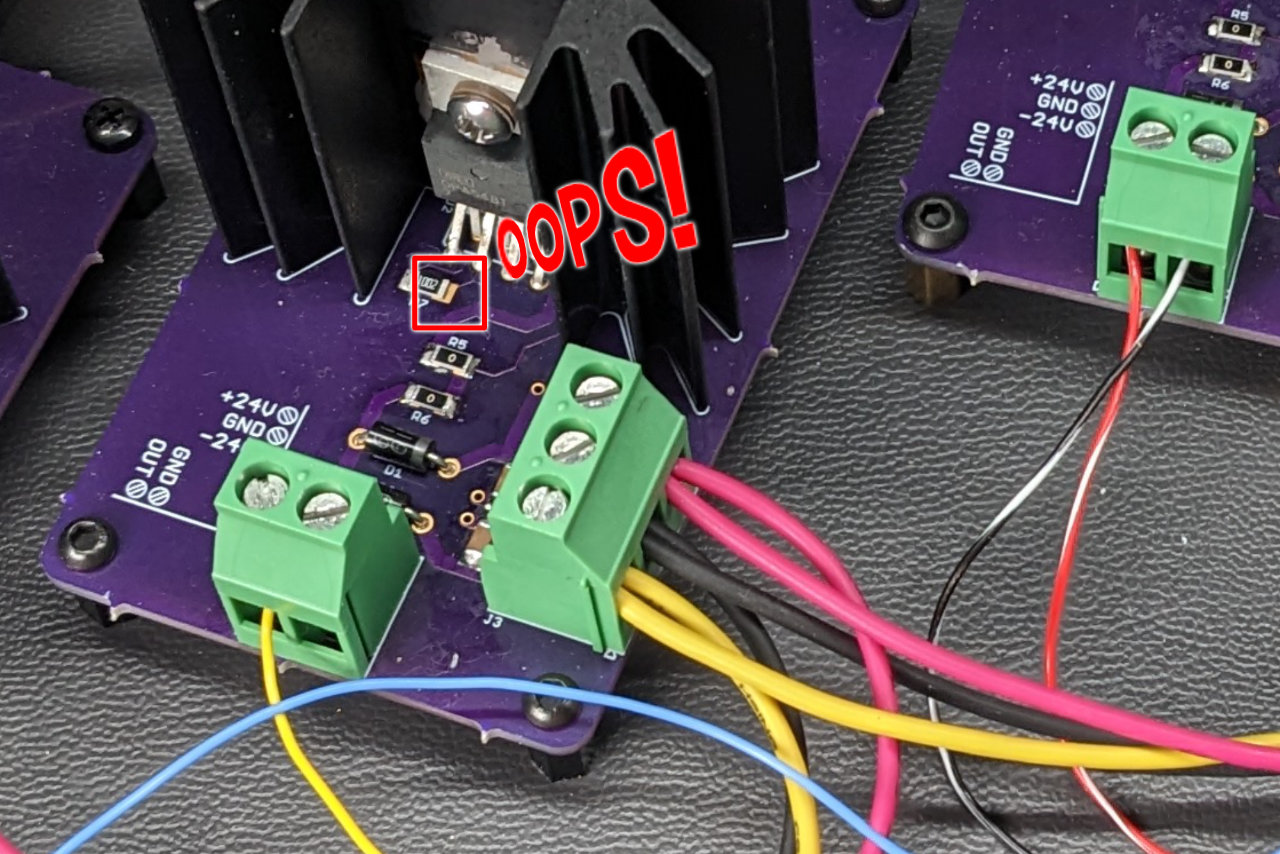
Missed soldering one terminal of the current limit set point resistor on one of the boards.
I initially had some issues with the synchro having two stable angles for any given angle entered into the terminal window. I traced this to a current limit set point resistor on one of the boards that only had one terminal soldered. As a result, one of the synchro format voltages would shut down under only a few mA of load rather than the rated 3A. Soldering the current limit set point resistor correctly fixed the issue and the synchro only has a single stable position for any entered angle.
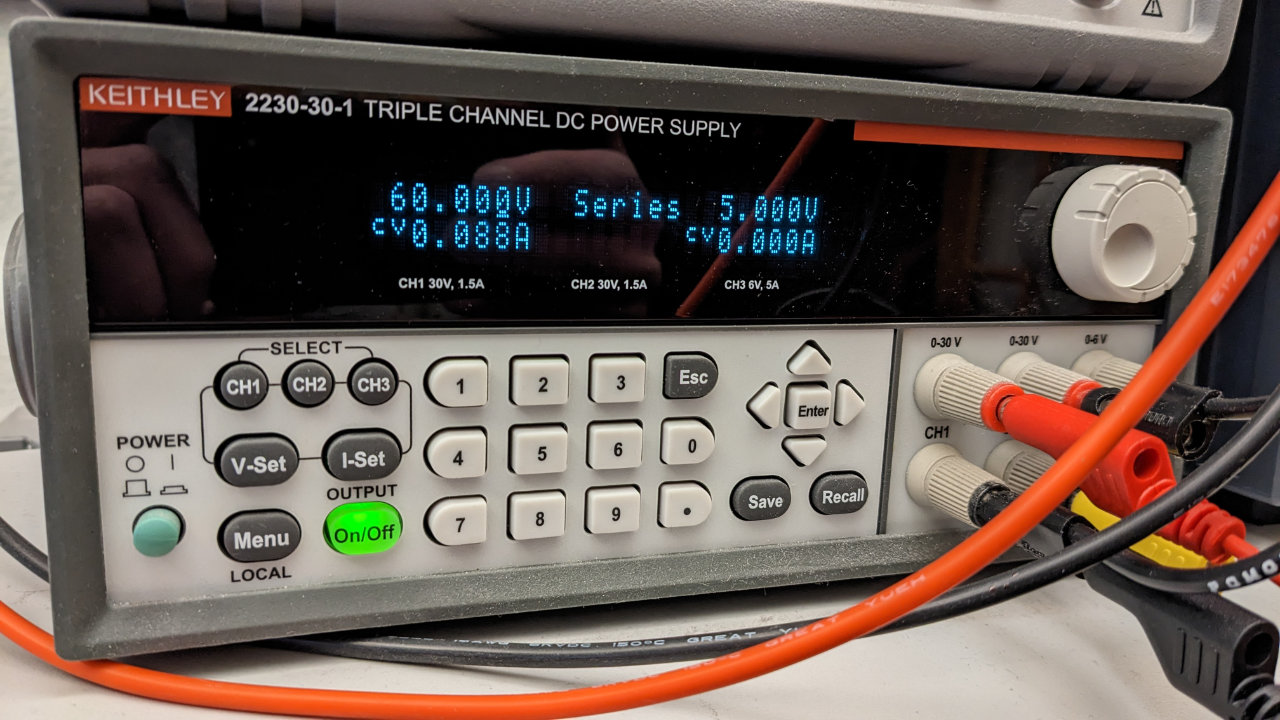
Voltage and current supplied to the completed project.
With the synchro at the entered angle, the system draws roughly 90 mA. In the photo, I have the power supply set for 60 V and series configuration to create a 30 V bipolar supply. I later reduced the voltage to 56 V in series yielding a 28 V bipolar supply and did not any experience any issues with the op amps running out of headroom. The current draw remained roughly the same.
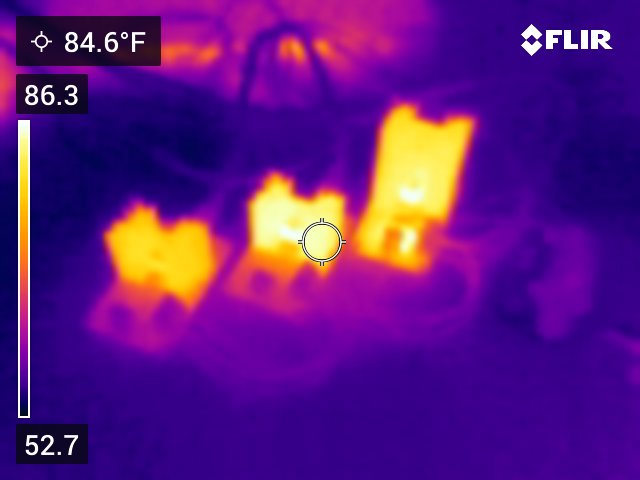
A thermal image of the power op amps and heat sinks.
A quick check of the op amps and heat sinks with the thermal camera revealed they run pretty cool and could likely be downsized.
Bonus content: Controlling a real, unmodified aircraft instrument!
I put together another short demo. In the video above, I’m controlling a real, unmodified aircraft radio magnetic indicator’s compass card from a PC using the digital-to-synchro converter! It’s 120° off but otherwise works perfectly. Note that the compass card is controlled by a control transformer in a servo loop rather than by a synchro receiver.
Final Thoughts
In this project, I demonstrated that it was possible to build a digital-to-synchro converter using modern hardware. At some point, I’d like to re-spin the boards to put all three op amps and the Raspberry Pi Pico on the same board. I would also be interested in obtaining a Scott configuration transformer to try to build a galvanically isolated version of the circuit.
Downloads
The board design files and software for this project are available in the digital-to-synchro directory of my avionics repository on Github.
References
Analog Devices: Synchro and Resolver Conversion Handbook, 1980
Data Device Corporation: Synchro/Resolver Conversion Handbook, 2009 (PDF)