
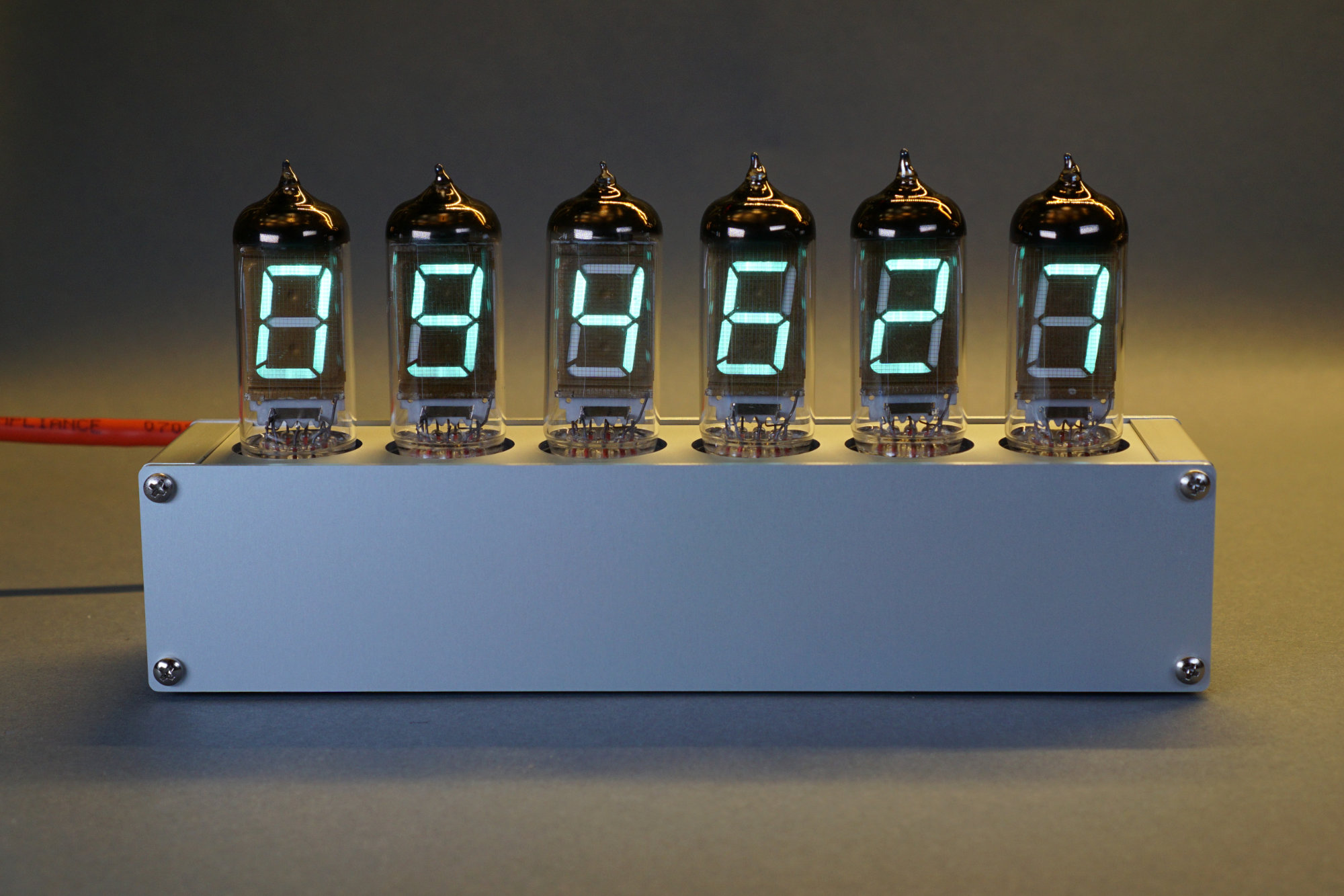
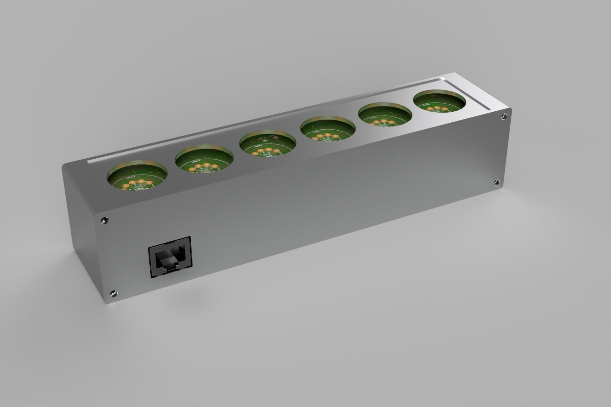
The completed and assembled PoE-powered vintage VFD tube clock.
This is a vintage VFD tube clock that uses Ethernet for both power and data. The power is provided using 802.3at PoE+ and a Molex PD Jack that contains both integrated magnetics and a PoE Type 2 PD controller. The IP stack runs on a Microchip PIC18F67J60 microcontroller that has an integrated Ethernet MAC and PHY. The IP stack includes DHCP, DNS, NTP, and LLDP functionality.
The clock powers up and receives its IP address and a DNS server address via DHCP. LLDP is used to negotiate 7.5 Watts of power. The clock performs a DNS lookup to get an NTP server address from pool.ntp.org. Once the clock has the address of an NTP server, it uses NTP to set the date and time. With the date and time set, the clock displays the time using the 6 VFD tubes and three MIcrochip HV5812 high-voltage display drivers. Once an hour, the clock corrects any drift using NTP.
Vacuum Fluorescent Displays

A modern vacuum fluorescent dot matrix character display module circa 2008.
Vacuum fluorescent displays occupy a niche in history between their high-voltage Nixie predecessors and their expensive-at-the-time LED successors. They can be identified by their relatively fast response times, wide viewing angles, and characteristic blue-green glow.
The dual-axis inclinometer photo above shows a relatively modern vacuum fluorescent display. This display is a drop-in replacement for a character LCD module. It’s visible at night, in bright sunlight, and from any angle unlike the LCD it replaced. This display module is circa 2008. Thisinclinometer was built to show the pitch and roll of my Jeep long before vehicles included this features in their instrument clusters.
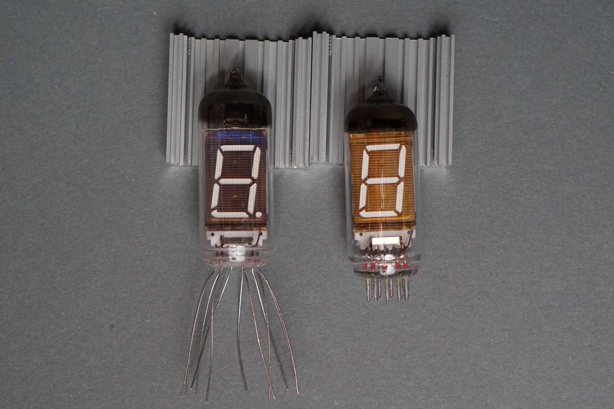
An IV-11 VFD tube from 1989 on the left and an IV-12 VFD tube from 1992 on the right.
This clock project uses even older VFD tubes. The tubes are available in a variety of formats. In the photo above are two styles of VFD tubes. The tube on the left is an IV-11 display tube from 1989. The tube on the right is an IV-12 display tube from 1991. The only real difference between these tubes is the IV-11 on the left has a right-hand decimal point and wire leads while the IV-12 tube on the right lacks a decimal point altogether and has pins to mount the tube in a socket.
A Nixie tube requires 170 V DC to drive the tube’s anode. Vacuum fluorescent display tubes only require 25 V DC. As a result, they’re much easier to drive. Both tubes have a grid, a heater, and an anode per display segment. The electrical requirements for each are displayed in the table below:
| Volts | Minimum Current | Nominal Current | Maximum Current | |
|---|---|---|---|---|
| Heater | 1.5 V | 90 mA | 100 mA | 110 mA |
| Grid | 25 V | 12 mA | — | 17 mA |
| Anode / Display Segment | 25 V | 3 mA | — | 5 mA |
With six tubes, the worst case heater current consumption is 6 tubes * 1.5 V * 0.110 A = 0.99 W. With six tubes, the worst case grid power consumption is 6 tubes * 25 V * 0.017 A = 2.55 W. With six tubes, the worst case segment power consumption is 6 tubes * 7 segments * 25 V * 0.005 A = 5.25 W. A six digit clock is then going to need a 1.5 V power supply capable of supplying 0.99 Watts and a 25 V power supply capable of supplying 7.8 Watts.
I decided to use the IV-12 tubes with the pins for sockets on their base. In the event of a mistake on one of my PCBs, I could unplug the tubes and re-use them on a corrected board. In the event of a failed tube, I could swap tubes on the project without significant PCB rework.
VFD Tube PCB Footprint
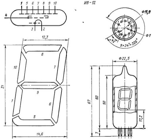
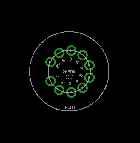
This is the only IV-12 tube diagram I could find showing the positions of the pins on the bottom of the tube.
After deciding on a tube to use for the clock project, the next step was to generate a schematic symbol and PCB footprint for the tube. I had a very hard time finding the diameter and spacing of the tube’s pins. I finally found a single low resolution image (reproduced above) on an eBay listing for the tubes. Of course, it doesn’t say if that’s a top or bottom view of the tube or which direction the front of the tube faces.
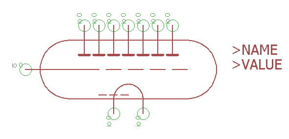
IV-12 VFD tube schematic symbol. I have no idea which anode pin corresponds to which display segment but I will be able to remap them in software so it doesn’t really matter.
I created a schematic symbol for the VFD tube. The left pin is the grid anode, the bottom two pins are the heater pins, and the top seven pins are the segment anodes.
After creating the schematic symbol, I created a PCB footprint for the part. I used the geometry from the data sheet and visual inspection of the base of the tube to create a Matlab / Octave script that creates an Eagle script to place the 11 pins and label them with their pin numbers. Here’s the Matlab / Octave code:
first = -(180-(360-306)/2);
increment = +34;
count = 10;
radius = 11.9 / 2;
text_radius = radius - 2;
drill = 1.95;

fprintf (1, 'grid mm;\n');
fprintf (1, 'change align bottom-center;\n');
fprintf (1, 'change size 32mil;\n');
fprintf (1, 'change font vector;\n');
fprintf (1, 'change ratio 16;\n');
fprintf (1, 'change drill %5.2f;\n', drill);

for i=1:count
  angle = first + (i-1) * increment;
  x = cos (angle / 180 * pi);
  y = sin (angle / 180 * pi);
  xp = x * radius;
  yp = y * radius;
  xt = x * text_radius;
  yt = y * text_radius;
  at = 90 + angle;
  %fprintf (1, "%4d %8.4f %8.4f\n", angle, x, y);
  fprintf (1, "pad '%d' round 0 (%8.4f %8.4f);\n", i, xp, yp);
  if (angle >= 0)
    fprintf (1, "text '%d' sr%d (%8.4f %8.4f);\n", i, round(at), xt, yt);
  else
    fprintf (1, "text '%d' r%d (%8.4f %8.4f);\n", i, round(at), xt, yt);
  endif
endfor
Running this code produces the following Eagle script:
grid mm;
change align bottom-center;
change size 32mil;
change font vector;
change ratio 16;
change drill  1.95;
pad '1' round 0 ( -5.3015  -2.7012);
text '1' r-63 ( -3.5195  -1.7933);
pad '2' round 0 ( -2.8846  -5.2040);
text '2' r-29 ( -1.9150  -3.4547);
pad '3' round 0 (  0.5186  -5.9274);
text '3' r5 (  0.3443  -3.9350);
pad '4' round 0 (  3.7445  -4.6240);
text '4' r39 (  2.4858  -3.0697);
pad '5' round 0 (  5.6900  -1.7396);
text '5' r73 (  3.7774  -1.1549);
pad '6' round 0 (  5.6900   1.7396);
text '6' sr107 (  3.7774   1.1549);
pad '7' round 0 (  3.7445   4.6240);
text '7' sr141 (  2.4858   3.0697);
pad '8' round 0 (  0.5186   5.9274);
text '8' sr175 (  0.3443   3.9350);
pad '9' round 0 ( -2.8846   5.2040);
text '9' sr209 ( -1.9150   3.4547);
pad '10' round 0 ( -5.3015   2.7012);
text '10' sr243 ( -3.5195   1.7933);
Running this script in the Eagle PCB library editor produced the bulk of the following footprint:
Finished IV-12 VFD tube PCB footprint.
After running the script, I added an outline of the tube, labeled the front, and added some notes about which pins should be connected to which supplies. While researching this project, I came across one note that said the displays appeared brighter when 1.5 V is connected to pin 2 and ground is connected to pin 3 rather than the other way around. I did not verify that guidance but decided to follow it anyway.
The drills for the pads are 1.95 or 2.00 mm in diameter. These holes accommodate Harwin H3161-01 pin sockets for 1 mm pins. These are press fit into the holes in the PCB then soldered into place. The tube pins are 1 mm in diameter and fit in these pins easily. I used 1.95 mm drills on the clock but would use 2.00 mm drills on future versions.
VFD Tube Socket Test Board
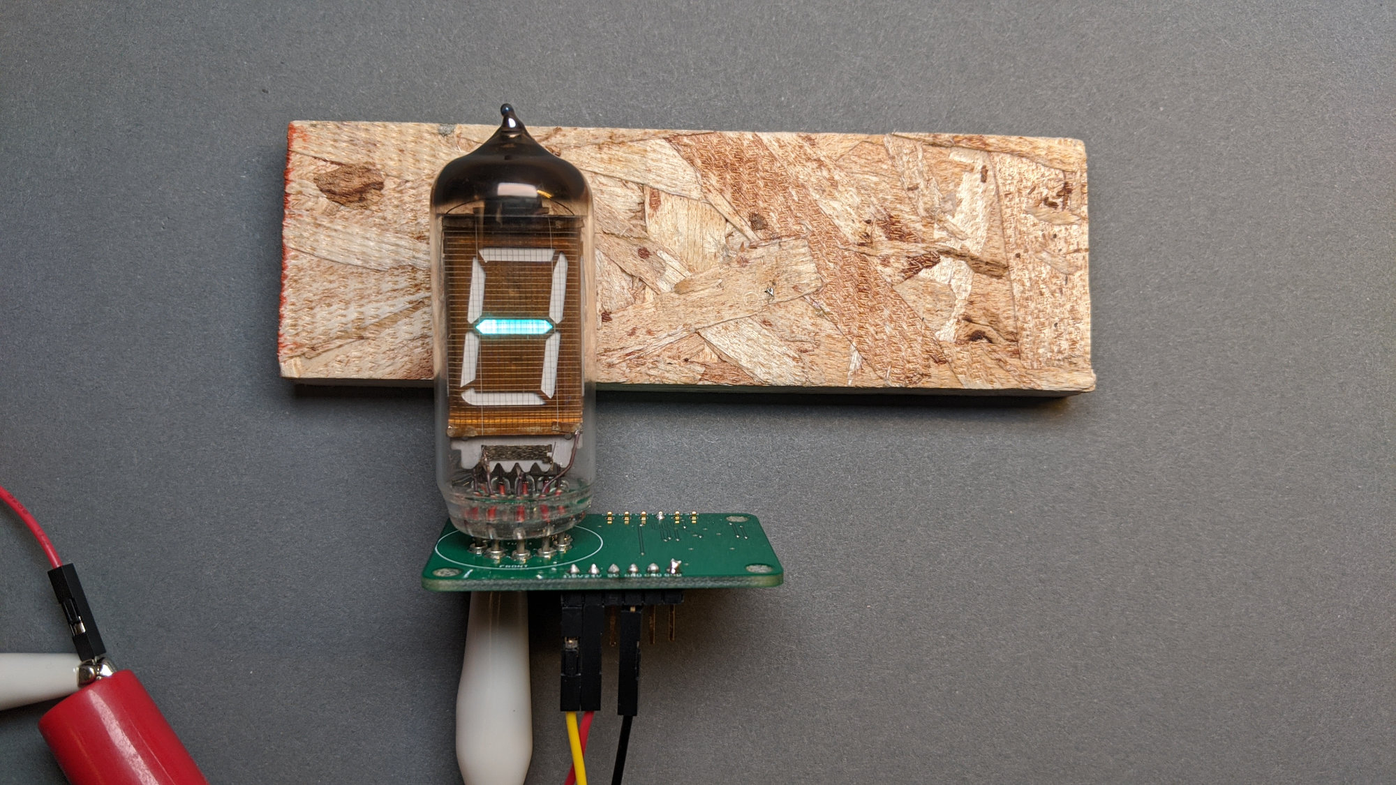
Test board to verify the placement of the sockets and how well the tube fits in the sockets.
After designing the schematic symbol and PCB footprint, I created a small test board to verify the placement of the sockets and how well the tube fits in the sockets. I powered on a segment on the tube to verify the location of the ground, heater, grid, and segment pins. Everything fit so I knew I had a good PCB footprint to use on the final clock board.
I included a Microchip HV5812 high-voltage display driver and Texas Instruments SN74LVC8T245 level shifter on the test board to test my circuit for controlling the tube but ultimately skipped testing the circuit before releasing the real boards.
Designing the Clock
Mechanical Design
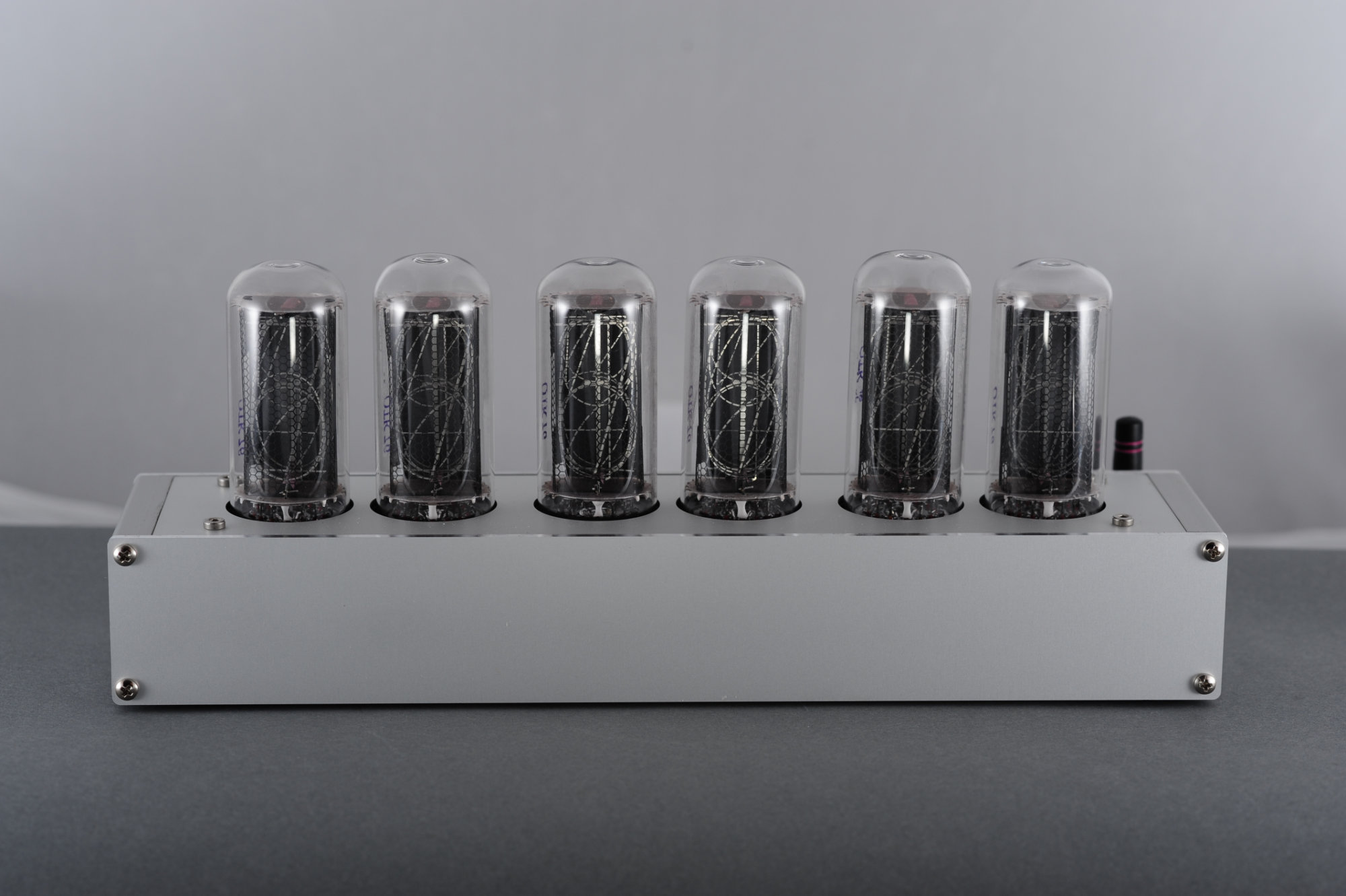
My six tube IN-18 Nixie tube clock from 2018.
With the ground work out of the way, it was time to start designing the clock. I wanted to give it a similar aesthetic to the six-digit IN-18 Nixie tube clock shown above that I designed in 2018. The IN-18 clock uses a CNC’d anodized aluminum enclosure with some extruded aluminum profiles on either end to hold everything together. The dimensions of the end profiles are shown in the diagram below.
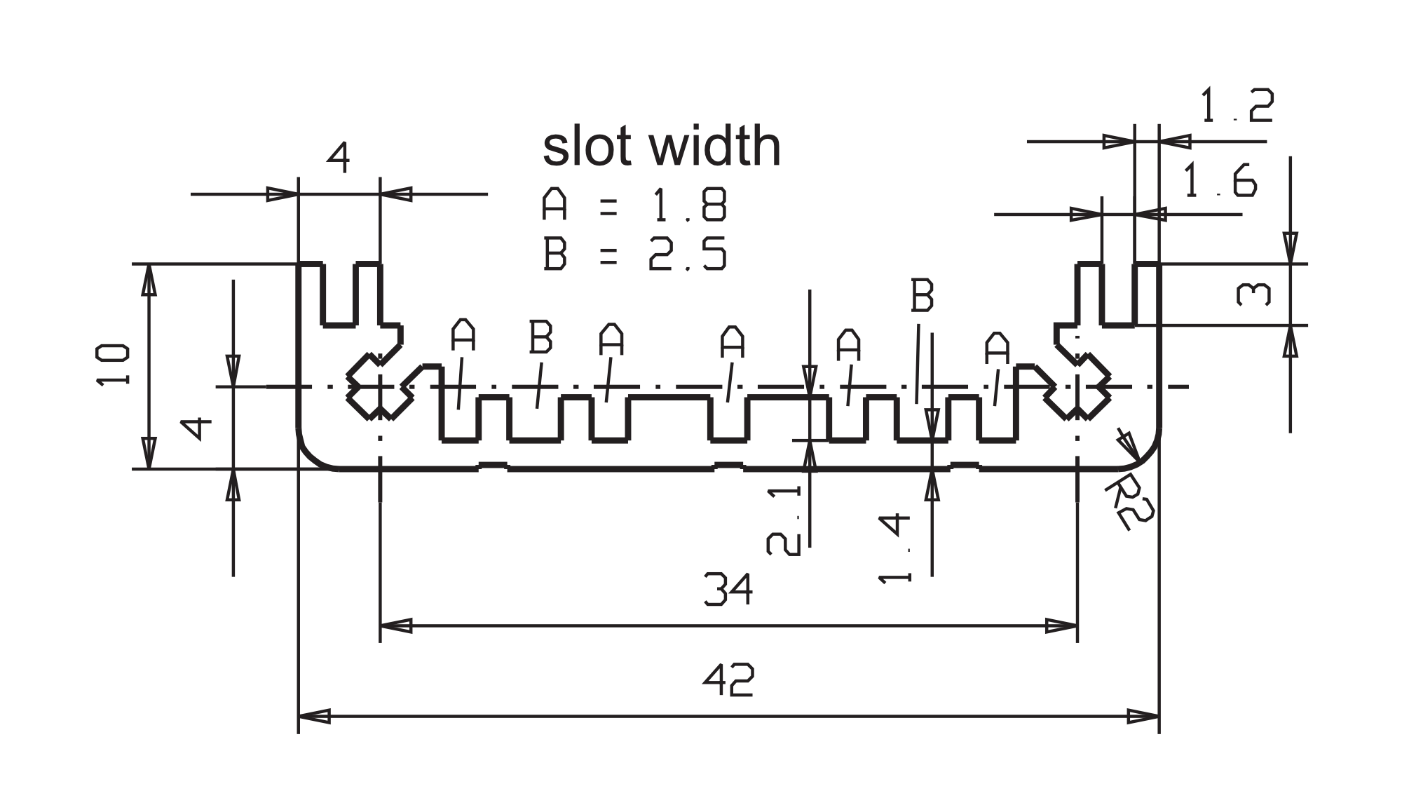
Front Panel Express enclosure profile #1 dimensions.
The “A” slots in the profiles are designed to hold 1.6 mm thick circuit boards. I wanted to decrease the depth and width of the VFD clock versus the Nixie clock. This would require using the slots in the profiles to hold the circuit board versus using screws through the top panel like I did on the Nixie clock. You can see the four screws to be eliminated on the top panel in the photo of the Nixie clock above.
Electrical Design
Next I turned my attention to the electrical hardware. The clock would require a microcontroller with Ethernet capable of using NTP to set the date and time, a display driver capable of sourcing 25 Volts, a bunch of power supplies, and use 802.3af/at for PoE/PoE+ for power.
Microcontroller
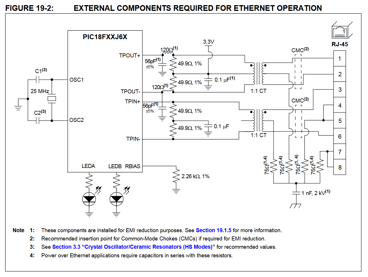
PIC18F67J60 minimal Ethernet circuit.
I decided to use the Microchip PIC18F67J60 for a microcontroller. The Microchip PIC18F67J60 includes both an internal Ethernet MAC and PHY and the Microchip Code Configurator includes software libraries for NTP. Most importantly, I had good luck with this microcontroller on my Ethernet-Powered Pixels project. This microcontroller requires a 3.3 V supply.
Display Segment Driver
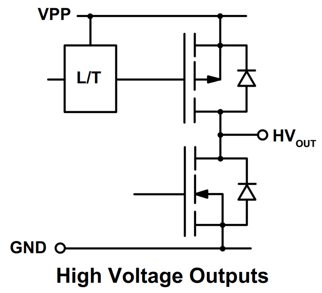
HV5812 high-voltage output configuration.
To drive the segments on the VFD tubes, I used a Microchip HV5812 20-channel serial-input display driver. These display drivers have full totem-pole outputs and are rated for 80 V. The data sheet implies each output is capable of sourcing at least 25 mA. Since each segment requires only 3 to 5 mA at 25 V, these parts are more than adequate for driving the VFD tube segments. One HV5812 would be used for every two tubes.
The only downside is these parts require a 5 V supply and their inputs are referenced to this supply. If these parts were capable of running from 3.3 V, that would have eliminated the need for a 5 V power supply and level translator in this design.
Power Supplies
This design requires four power supply voltages. The tubes require 25 V and 1.5 V, the HV5812 drivers require 5 V, and the microcontroller requires 3.3 V. The 1.5 V, 3.3 V, and 5 V supplies will be powered from the 25 V supply. The 25 V supply will be powered from the 37 to 57 volt PoE supply.
I used CUI point-of-load, non-isolated DC/DC converters for the 1.5 V, 3.3 V, and 5 V supplies. The 3.3 V supply is a through-hole V7805-500 module. For the 1.5 V and 5 V supplies, I needed a shorter package than the V780x-500 and V780x-1000 modules so that the modules could fit between two boards separated by 11 mm. I used a V78E01-1000-SMT and V7805-500-SMT for the 1.5 V and 5 V supplies respectively. These are only 8.25 mm tall so they’ll easily fit between the two boards.
For the 25 V supply, I used a CUI PDQE20-Q48-S24-D isolated DC/DC converter. This module is a 24 V, 20 W converter and has a wide input voltage range of 18 to 75 V that will work with the PoE supply voltage of 37 to 57 V. This supply also has an adjustment input for fine tuning the voltage output. I ran through the math on the data sheet and figured with a resistor somewhere in the range of 55k, I could adjust the voltage output up to 25 V.
802.3af PoE / 802.3at PoE+ Power
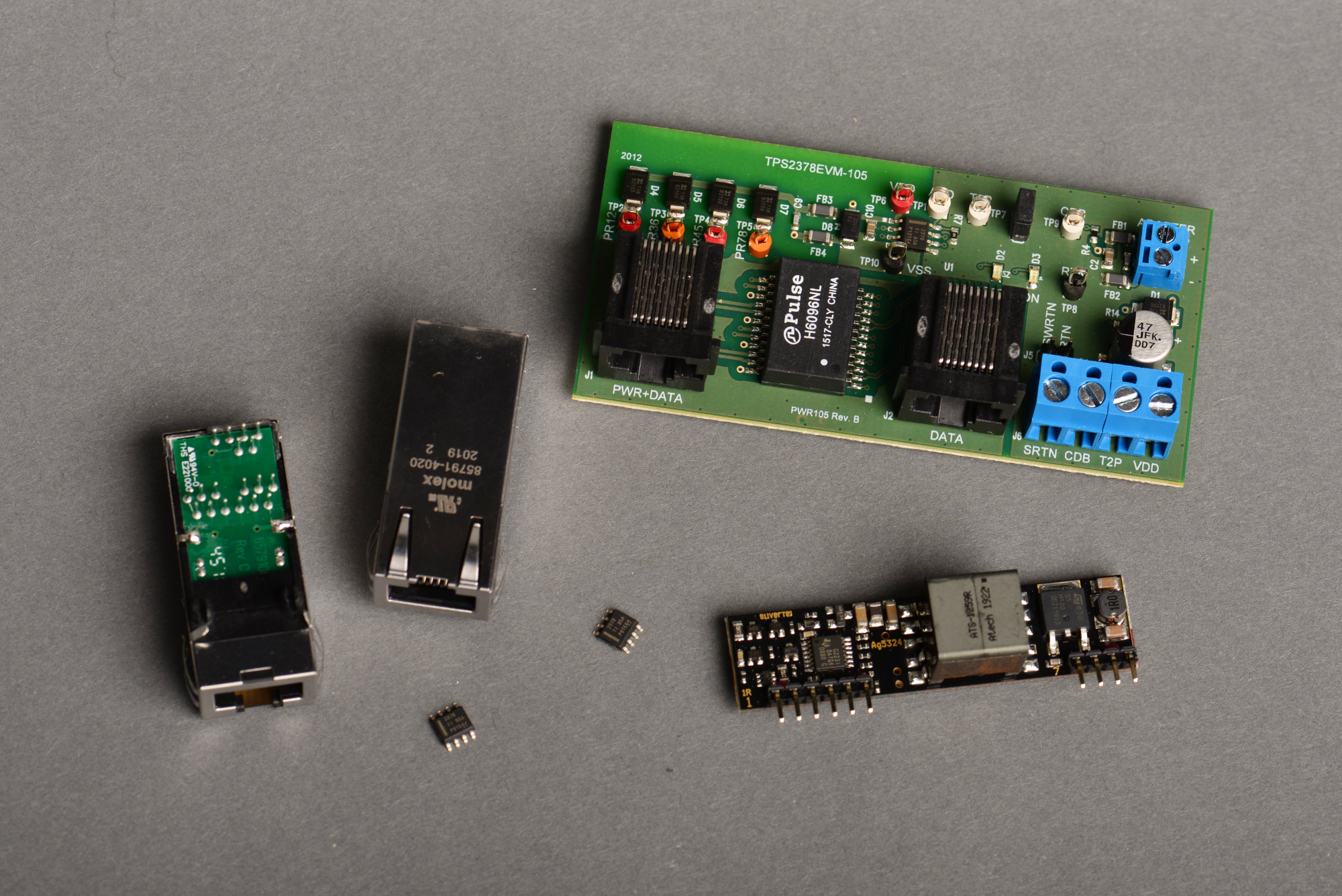
A bunch of different PoE+ PD components including two Molex PD jacks, two TI TPS2378 ICs, a TI TPS2378 evaluation board, and a Silvertel PoE+ PD 24 VDC module.
For this project, I decided to use a Molex 85791-4020 PD Jack for the 802.3at / PoE+ functionality. This Ethernet jack contains both integrated magnetics and Type 2 / Class 4 PoE+ classification circuitry. This one jack, shown on the left in the photo above, replaces most of the components on the evaluation board shown in the top-right of the photo.
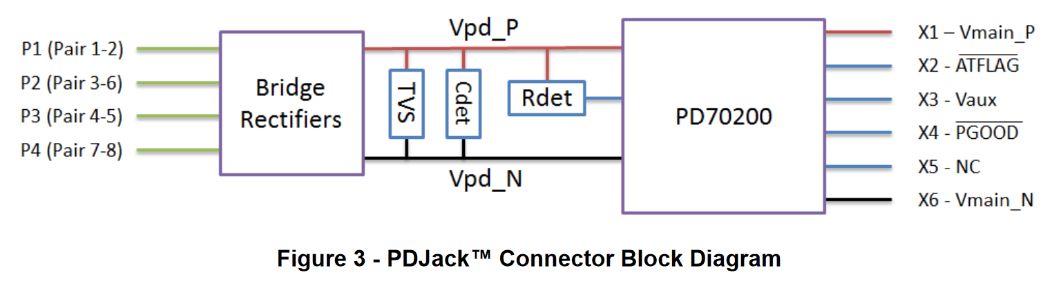
Molex 85791-x020 PD Jack block diagram.
The jack, in addition to the integrated Ethernet magnetics, contains all the circuitry required to perform 802.3at / PoE+ classification. This includes the bridge rectifiers, transient suppression diodes, detection capacitance, detection resistance, and an integrated Microchip PD70200 PoE classification IC. The block diagram from the datasheet is shown above. These jacks are bulky and expensive but for a one-off, hand-built prototype like this VFD clock, the reduction in parts count and assembly time was worth it to me.
Power / Control Board Function Split
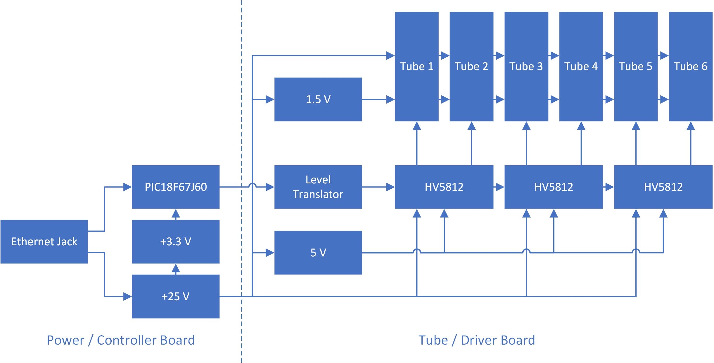
Block diagram of the clock project. The power / controller board contains the functions left of the dotted line. The tube / driver board contains the functions right of the dotted line.
Based on my experience designing the Nixie IN-18 clock, I knew the tube sockets, segment drivers, microcontroller, and power supplies would not fit on a single board and a two board stack would be required to hold all the components.
I decided to place the PoE and microcontroller circuitry and the 25 V and 3.3 V power supplies on a power / controller board and the level translator, segment drivers, tube sockets, and 1.5 V and 5 V power supplies on a tube / driver board. The boards are connected together using headers. The headers supply 25 V, a SPI interface, and the reference voltage for the SPI interface from the power / controller board to the tube / driver board.
This split would prove advantageous during board bring up because the power / controller board contains everything needed to run the microcontroller and the tube / driver board contains everything needed to power and control the tubes with a single 25 V supply and a SPI interface.
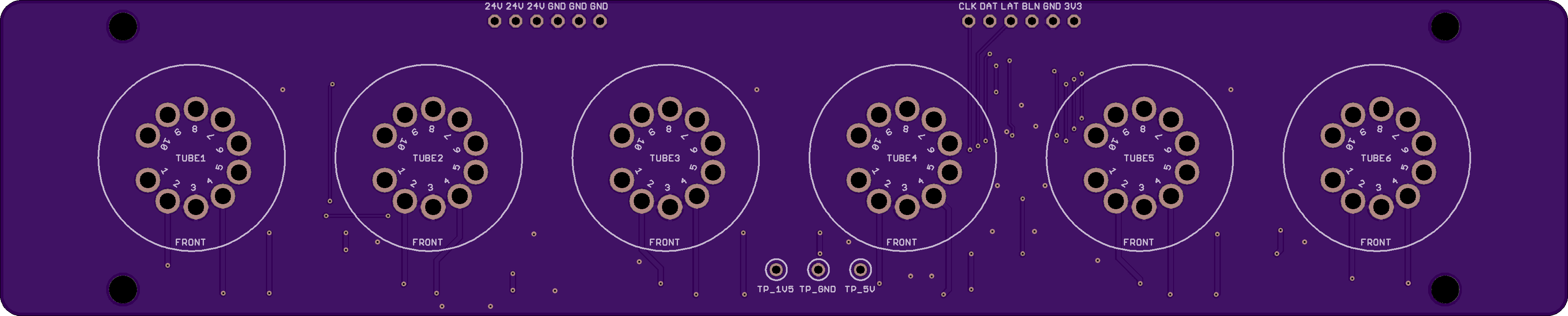
Tube / Driver Board Design
Schematic
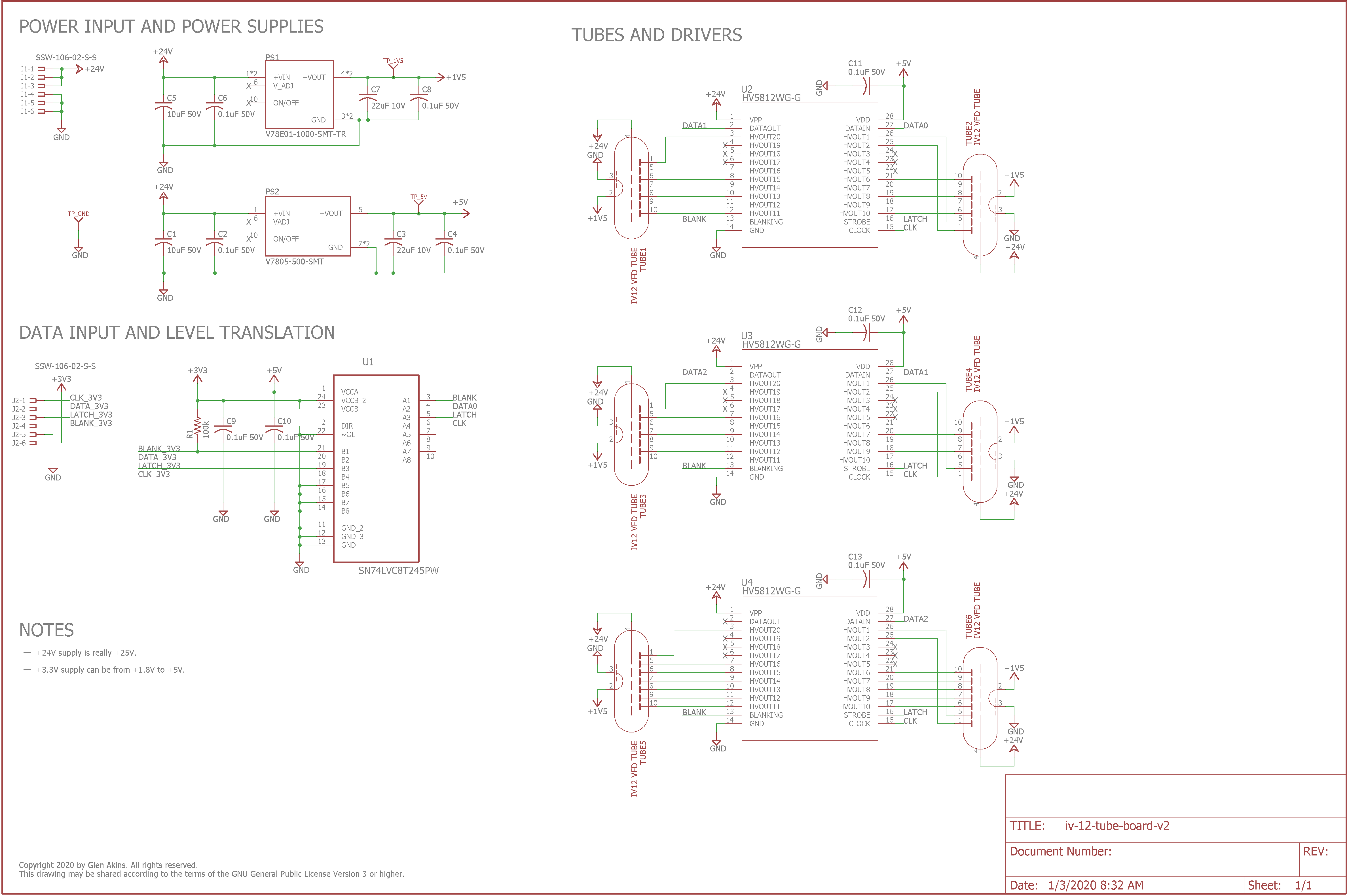
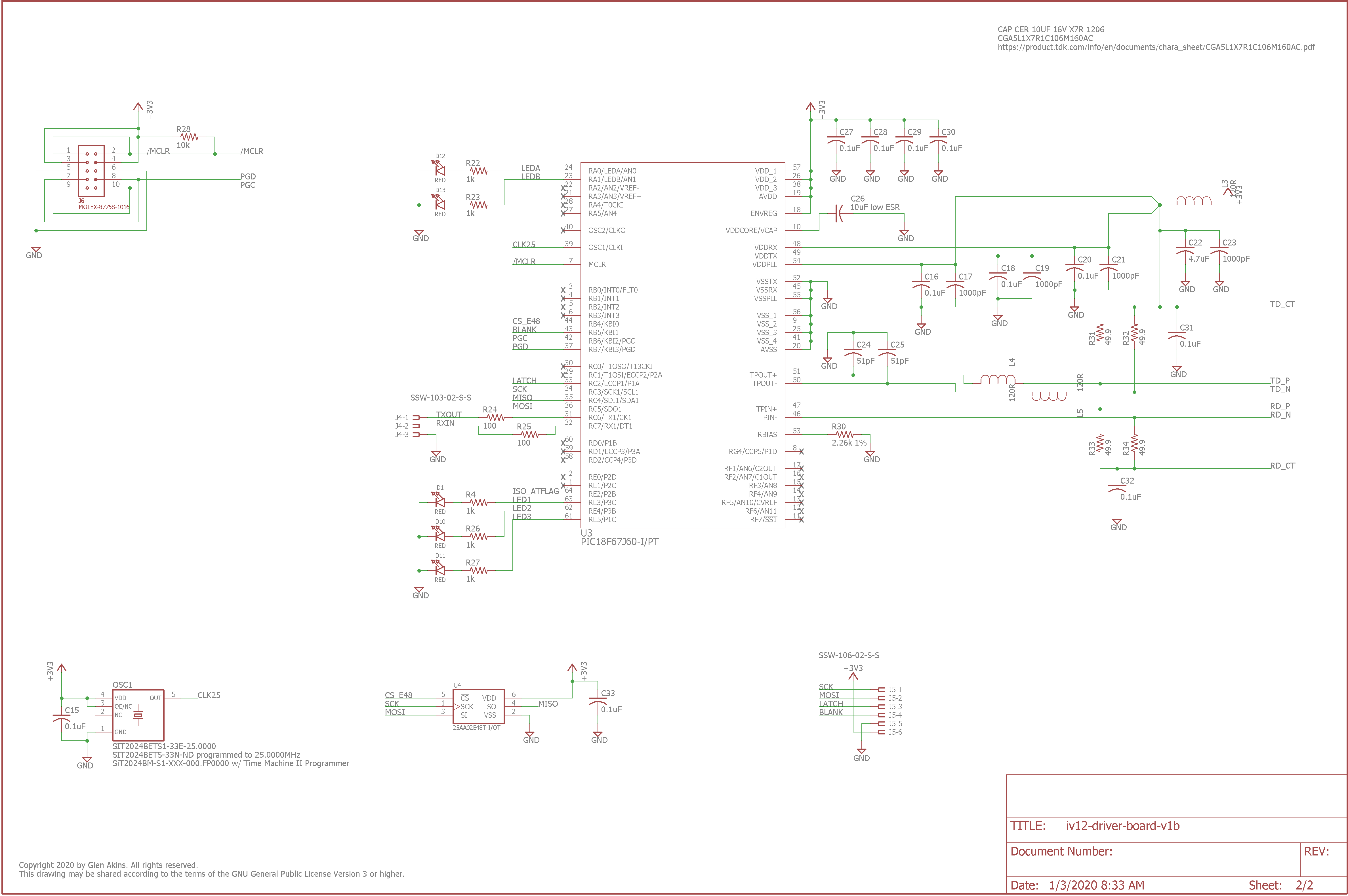
Schematic of the tube / driver board.
The schematic for the tube / driver board is shown above. It consists of three main sections: power input, data input, and the tubes and drivers.
The main power input is 25 VDC on J1. This voltage feeds the 1.5 V and 5 V converters to generate the voltages needed for the tubes’ heaters and the display drivers.
The data input on J2 consists of clock, data, latch, and blank signals. The logic levels of these signals are referenced to the voltage on J2-6 which can range from 1.8 to 5 V. In the case of our design, this is 3.3 V. This board could be used unmodified with a 5 V output microcontroller like the one on an Arduino by connecting J2-6 to +5 V instead of +3.3 V.
The tube drivers are Microchip HV5812 serial input high-voltage display drivers. The data signals are daisy chained between the three parts while the clock, latch, and blank signals are connected in parallel to all the parts. The tubes use the tube library symbol and footprint previously designed and tested on the tube socket test board.
Board
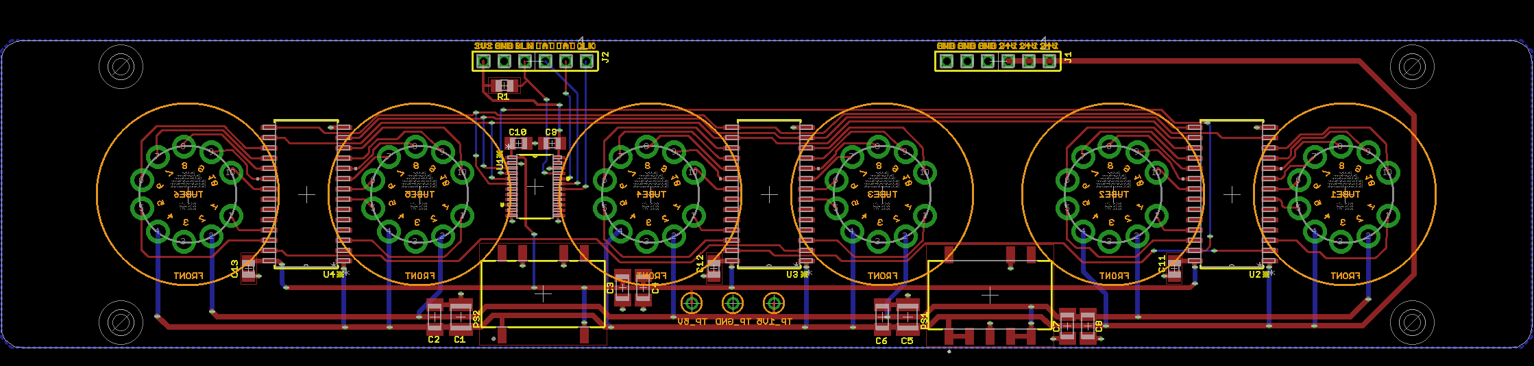
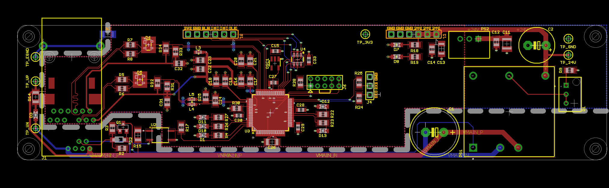
Finished tube / driver board layout.
Once the schematic was done, I designed a board in Eagle PCB. The tube pin sockets are located on the bottom of the board and the tubes extend into the screen with their fronts facing toward the bottom of the screen. The power supplies, display drivers, connectors and passives are located on the top of the board. After the design was done, the board’s width was extended to mount the board in the slots on the extruded aluminum profiles that form the sides of the enclosure.
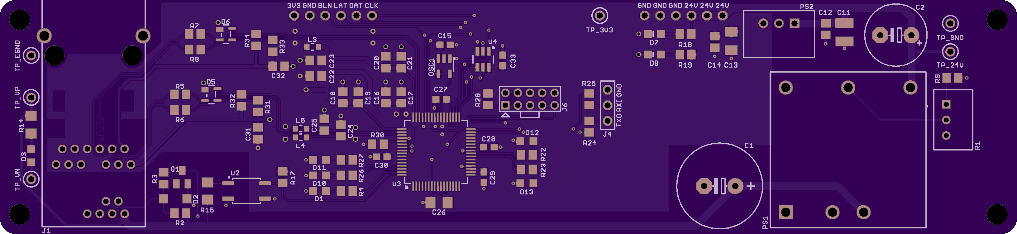
Tube board top.
I uploaded the design files to OSH Park and checked the board renders. Above is a render of the top side of the board.
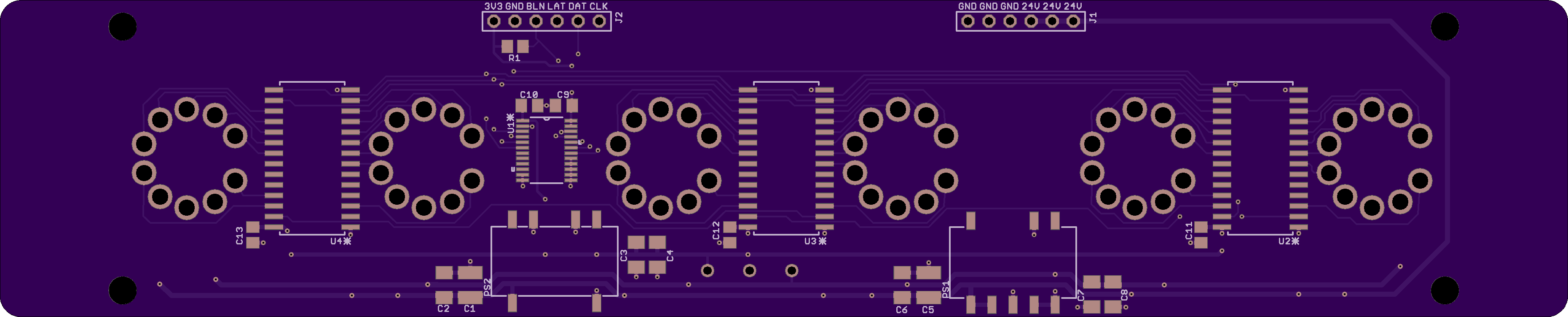
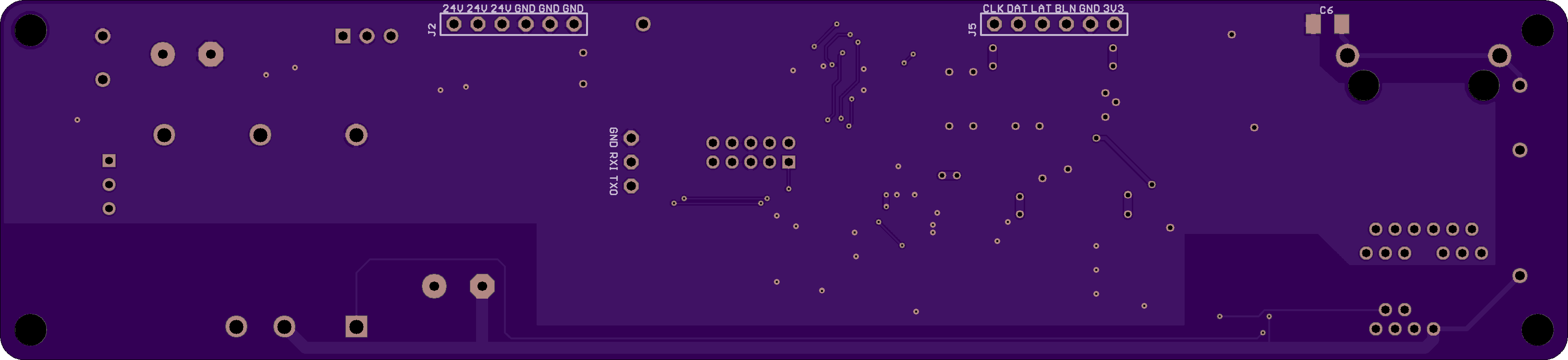
Tube board bottom.
Above is a render of the bottom side of the board. Once I was happy with the renders and had verified the boards and their components fit in the enclosure using Fusion 360, I placed an order for the boards at OSH Park.
A Complication and Another Test Board
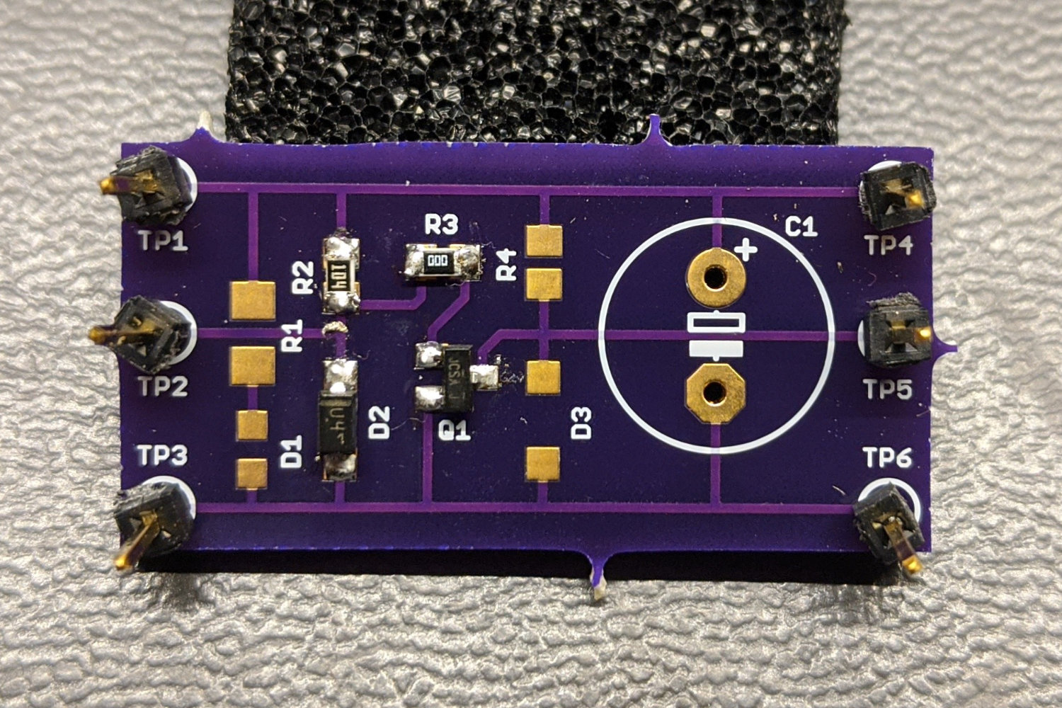
Open-drain, active-low power good to open-drain, active-low converter disable test board. Rated for 60 V operation.
One wrinkle to be solved before designing the power / control board was how to connect the Molex PD jack’s open-drain, active-low power good signal to the 24 V DC/DC converter’s active-low converter disable input.
The PD jack pulls its power good output low to indicate that the power is good and the external DC/DC converter should be enabled. The DC/DC converter has a converter disable input that disables the converter when it is pulled low.
I needed a circuit that will hold the converter disable input low while the power good signal is not pulled low and will release the converter disable input when the power good signal is pulled low. And the only power supply rail available is the 37 to 57 V PoE power.
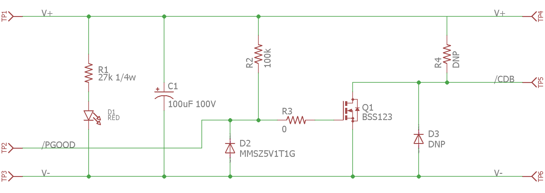
Open-drain, active-low power good to open-drain, active-low converter disable test board schematic. Rated for 60 V operation.
I solved this problem by designing the circuit shown in the schematic above. Ignore R1, D1, C1, D3, and R4. When /PGOOD is open, it’s pulled high by R2. Zener diode D2 limits the voltage when /PGOOD is pulled high to 5.1 V so as not exceed Q1’s maximum VGS. In this case, Q1 conducts and connects the /CDB output to ground thus disabling the DC/DC converter. When /PGOOD is pulled low, the gate of Q1 is pulled low and Q1 stops conducting. The allows the /CDB output to float high and enables the DC/DC converter.
To test the circuit, I built a small test board. Only D2, R2, R3, and Q1 were stuffed on the test board. I connected the V+ and V- rails on the test board (TP1 and TP3 respectively) to a bench power supply set for 60 V. I connected the power outputs (TP4 and TP6) to the converter’s DC input and the /CDB output (TP5) to the converter’s converter disable input.
I then turned on the bench power supply and verified the converter’s output was disabled. After placing a jumper between /PGOOD (TP2) and V- (TP3), I verified the converter’s output was enabled. I disconnected and connected the jumper a few more times to verified the converter’s output was on only when the /PGOOD signal was connected to V-.
Power / Controller Board Design
Schematic
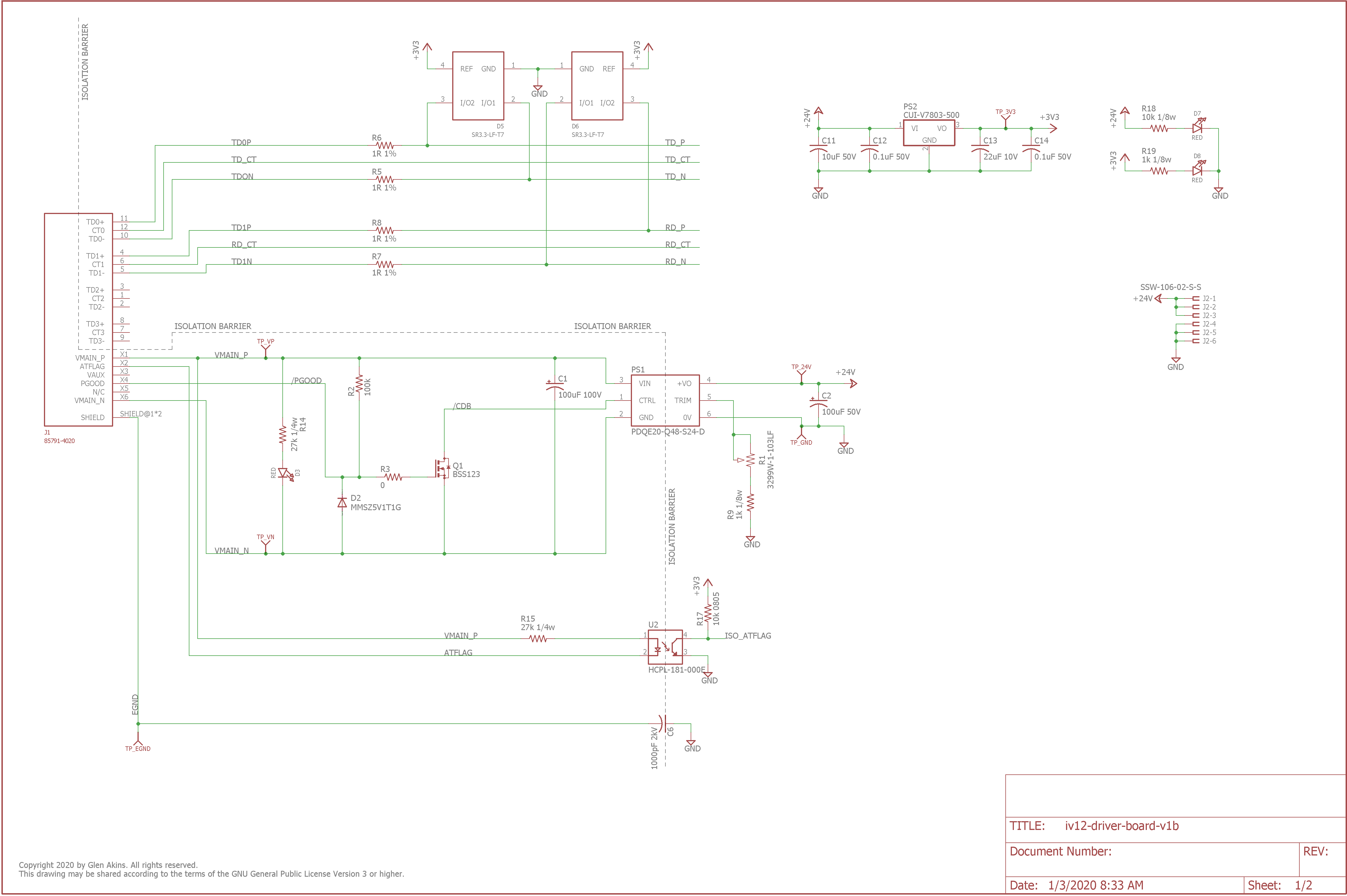
First page of the schematic for the power / control board.
After designing the tube board and verifying the converter enable/disable circuit, I designed the schematic for the power / control board. Page 1 of the schematic is shown above and page 2 of the schematic is shown below.
Second page of the schematic for the power / control board.
This is basically the same circuit that I used for the Ethernet-powered pixels project but with the following changes:
- Ethernet jack, magnetics, and PoE classification circuitry have been replaced by the Molex PD Jack.
- The addition of the /PGOOD to /CDB active-low, open-drain inverter circuit.
- The 5 V, 20 W converter is now a 24 V, 20 W converter and its adjustment pin is connected to a variable resistor to permit adjustment of the output voltage up to 25 V.
- The 25 V and 3.3 V power rails, the SPI data and clock, and two GPIO signals are routed to header sockets that connect to the tube / driver board.
After the schematic was complete I moved on to designing the board.
Board
Finished control board layout.
On the initial revision of the board, I had the power supply circuitry next to the Ethernet jack and the microcontroller on the right hand side of the board. I decided the Ethernet traces between the jack and the microcontroller were too long so I moved the microcontroller to the center of the board and moved the power supply circuitry to the right-hand side of the board.
The thick dashed white line is a 56 mil isolation gap between the PoE power circuitry and the isolated microcontroller circuitry. This board is less wide than the tube / driver board because it needs to fit between the extruded aluminum side profiles rather in the slots on the profiles.
Controller board top.
I uploaded the design files to OSH Park and checked the board renders. Above is a render of the top side of the board.
Controller board bottom.
Above is a render of the bottom side of the board. Once I was happy with the renders and had verified the boards and their components fit in the enclosure using Fusion 360, I placed an order for the boards at OSH Park.
Enclosure Design
Rear view of the PoE-powered VFD tube clock enclosure.
The enclosure was designed using Front Panel Express’s software, their enclosure design manual, and the side profile enclosure macros built into the software. Once the enclosure was designed, I exported DXF files from their software and imported them into Fusion 360.
Inside Fusion 360, I extruded the shapes in the DXF files into bodies with their actual thicknesses and assembled the enclosure. I used Eagle PCB’s integration with Fusion 360 to import my empty circuit boards into Fusion 360 and placed the boards in the enclosure. Rather than model all the components on the board, I placed only the larger components that I thought might cause interference with the boards or the enclosure.
Enclosure design showing boards and their position in the enclosure.
Above is an image captured in Fusion 360 showing the enclosure, the placement of the boards inside the enclosure, and the placement of the lager components on the boards. Once I was happy with the enclosure design, I ordered the panels from Front Panel Express.
Enclosure Test Fit
Test fit of the enclosure panels, boards, and Ethernet jack.
After what seemed like an eternity, my enclosure panels and circuit boards arrived. I assembled the enclosure but left the front panel off then bolted the two boards together using M3 x 11 mm spacers and placed the Ethernet jack in its footprint on the power / control board. I slid the boards into the top slot of the enclosure and the Ethernet jack aligned perfectly with the cut out in the rear panel.
I failed to account for the tabs that OSH Park uses to panelize their customers’ boards together though. I had to use a file to file down the tabs to get a smooth edge on all the boards for them to fit in the enclosure. Next time I would bring each of the two long edges in 0.25 mm (0.5 mm narrower total) to cut down on the amount of filing I had to do and account for OSH Park’s manufacturing tolerances.
Tube / Driver Board Bring Up
I decided to stuff and bring up the tube / driver board first. I populated the ICs, followed by the DC/DC converters, passives, and pin headers. While soldering these, I taped off the pin socket holes so I wouldn’t accidentally drag the iron across them and fill any of the holes with solder. Cleaning them out well enough to insert the socket pins would be difficult.
Once all the other parts were soldered on the board, I pushed the 60 pin sockets through the holes on the board. I had to use a make shift tool (broken chopstick) and some force to seat them in their holes. Next time, I’d use at least a 2.00 mm drill instead of a 1.95 mm drill for the holes to make inserting the pin sockets easier. Lastly, I soldered the pins in place.
To bring up and test the board, I used my Keysight bench power supply and a Particle Photon board. I set the bench power supply to supply 25 V at 100 mA and 5 V at 350 mA. I connected the 25 V to the power header on the tube / driver board and the 5 V to the micro USB connector on the Particle Photon.
I then connected the ground, SPI clock and data lines, and two GPIOs from the Particle Photon to the data connector on the tube board. I also connected the Particle Photon’s 3.3 V output to the 3.3 V input on the data connector to supply the input side of the level translator IC on the tube / driver board.
With the hardware connections complete, I turned to writing some software to permit the display of numeric strings on the tubes. The hardest part of this was mapping the 64 bits sent using the SPI interface to the 42 segments of the VFD tubes.
After figuring out the mapping, I wrote a function to display a numeric string on the tubes and registered it with the Particle Cloud. I could then use the Particle Console to send a string like “123456,” “——,” or “******” to display on the tubes. Any character place with a ‘*’ shows the spinning segments animation. The result of this effort is shown in the video above. Success!
Power Supply Bring Up and Adjustment
Power supply bring up successful!
After bringing up the tube / driver board successfully, I decided it was time to focus on the PoE and power supply circuitry. I stuffed the PoE and power supply components on the power / control board and attached a DMM to the +24 V and ground test points.
I connected the board to my Ethernet switch. After a second or two, the LEDs lit indicating the 24 V and 3.3 V supplies were operating. I used a small screwdriver to adjust the 25-turn variable resistor until the DMM read 25 volts. I then moved the DMM to the +3.3 V test point and verified the 3.3 V supply was really 3.3 volts.
Power / Control Board Bring Up
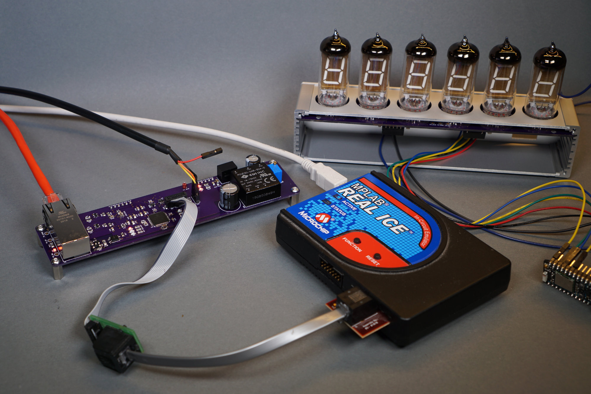
Power / control board microcontroller bring up successful!
Finally it was time to stuff the microcontroller and Ethernet parts on the power / control board. This is a tedious process because of the sheer number of passives. To aid in the process, I put the reference designators from the schematic in the customer data field when placing my Digi-Key order. This way each of the bags of passives was labeled with where they went on the circuit board. Genius.
After stuffing the board, I connected my MPLAB REAL ICE programmer and a 3.3 V serial cable to the board and downloaded the software from the Ethernet-powered pixels project to the board. I watched on the serial console as the board booted and obtained an IP address via DHCP from my router.
This was enough to prove almost all of the hardware worked. I connected the boards together and placed them inside the enclosure. I left the front of the enclosure off so that the serial cable and debugger could stay connected. It was all software now.
The Software
I used the Microchip Code Configurator to build a new project for the PIC18F67J60 microcontroller. I enabled all the Ethernet protocols this time: DHCP, DNS, UDP, TCP, NTP, and LLDP. To make the code that handles the interaction between the display tubes and the IP protocols easier to follow, I moved some of the higher-level code that deals with the sequencing of DHCP, DNS, NTP, and LLDP operations out of the network_manage function and in to the main function.
At boot, the software initializes the microcontroller’s peripherals, turns all the VFD tube segments off, and reads its Ethernet MAC address from a Microchip 25AA02E48 serial EEPROM with built-in globally unique Ethernet MAC address. After initialization is complete, the software spins the segments on the tubes until an IP address and DNS server IP address are assigned to the clock using DHCP. The software then displays the IP address twice and the DNS server IP address twice. The video above shows an early version of the software that gets an IP address for the clock via DHCP and displays it three times.
While the IP addresses are scrolling, the software is performing a DNS query to pool.ntp.org to get the IP address of an NTP time server. Once received, the NTP server IP adresss is displayed and the NTP server is queried for the current date and time. The received date and time is set then updated once per second using the 25 MHz SiTime MEMS oscillator for the time base.
The software applies time zone and daylight savings time correction to the received time and scrolls that across the tubes. After two scrolls of the date and time, the clock goes into “be a clock” mode where it displays the current TZ and DST corrected time on the tubes until the next reboot. Once an hour, a new NTP server is requested from pool.ntp.org and the time is re-synchronized.
The Finished Clock
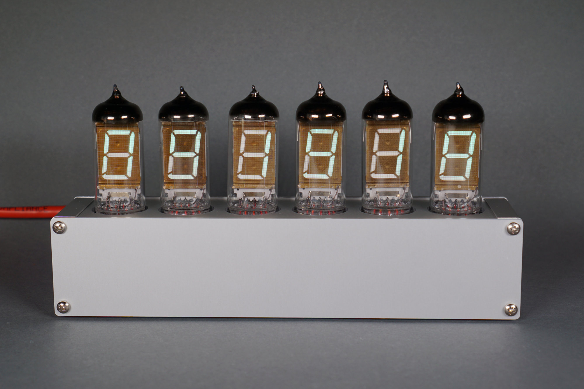
Finished and assembled clock. Front view.
Front view of the finished clock with the Ethernet cable connected.
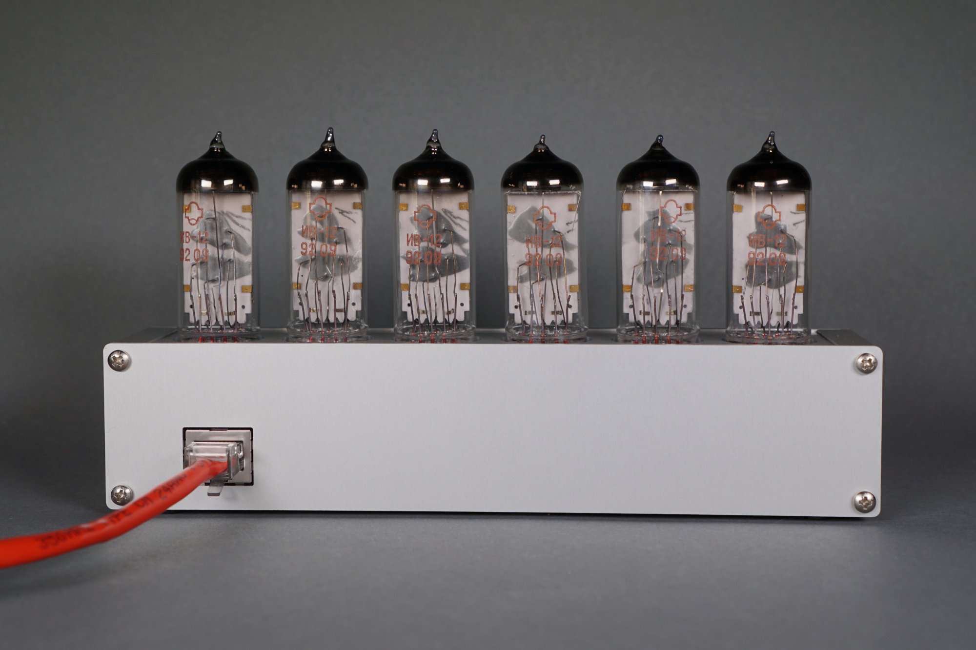
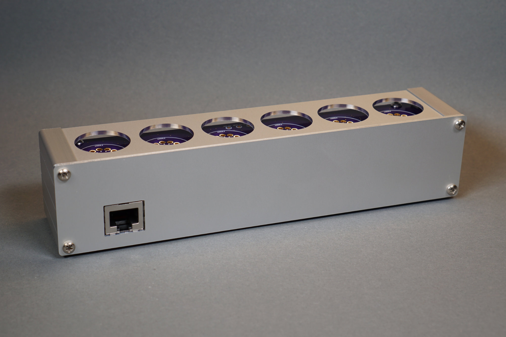
Finished and assembled clock. Rear view.
Rear view of the finished clock with the Ethernet cable connected.
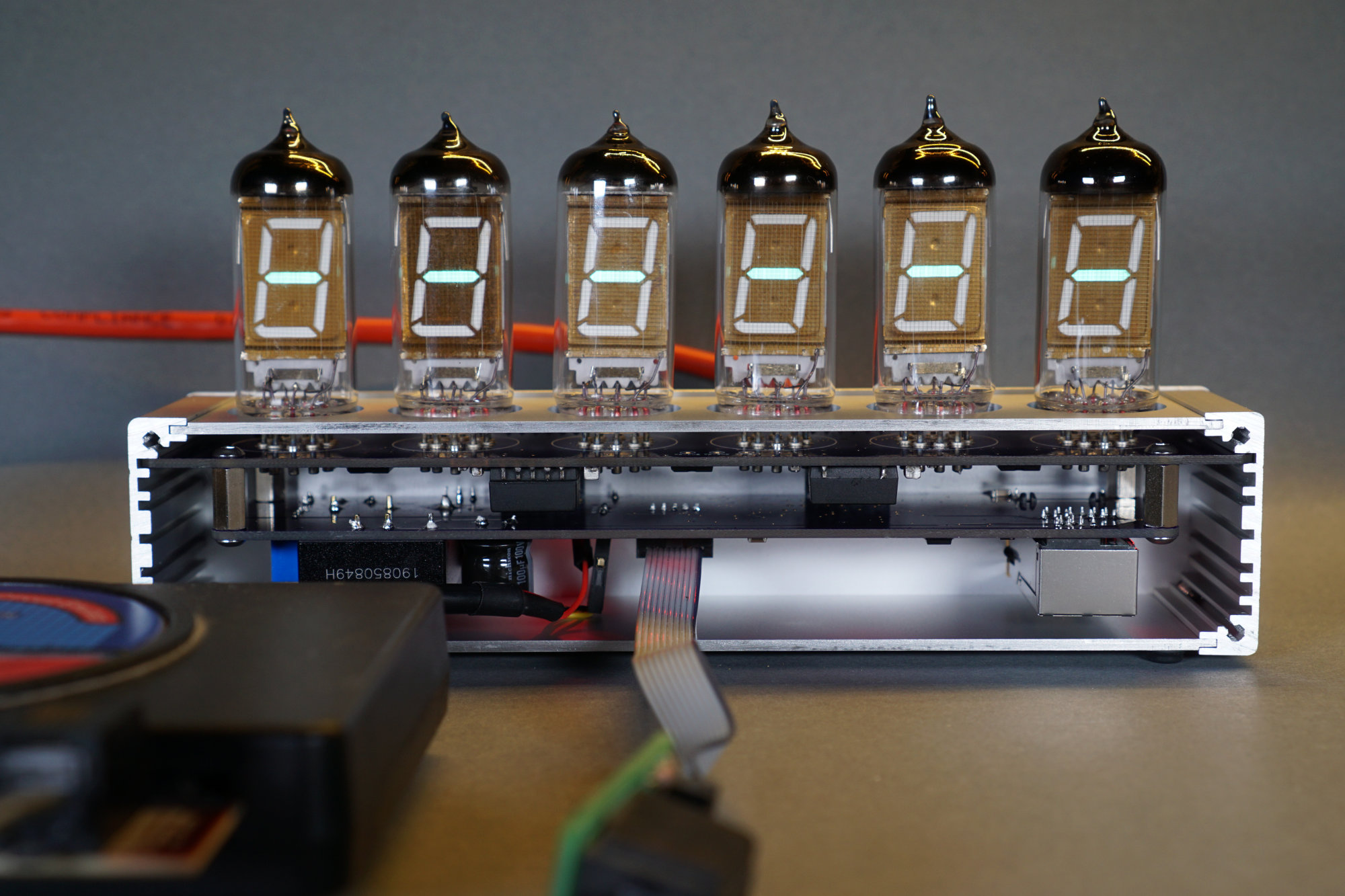
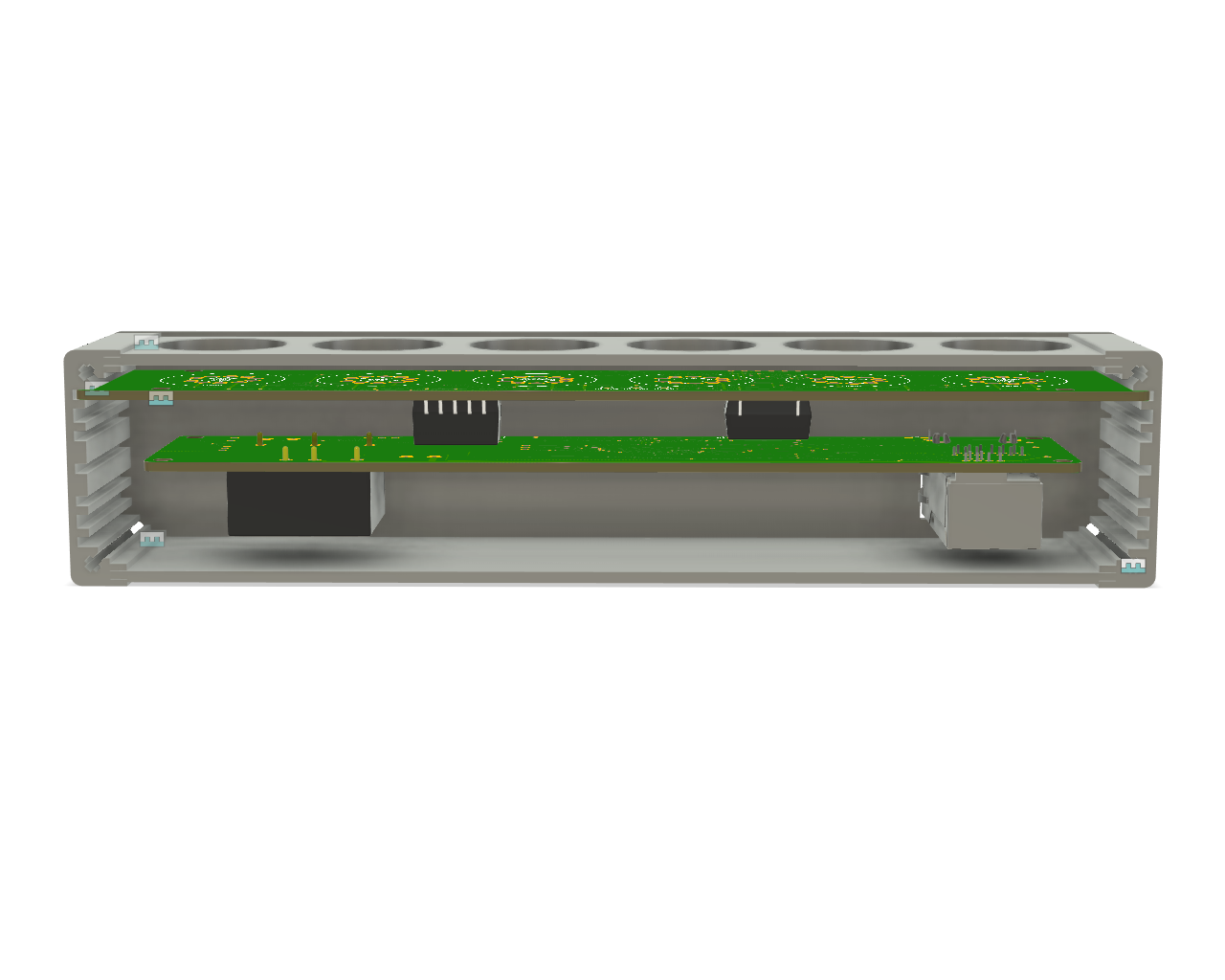
Internal view of the clock with the debugger and serial console cable still connected.
Interior view of the finished clock with the Ethernet cable connected.
Ideas for the Future
I’m thinking about upgrading the power / control board to use an ATSAMD21 with the Wiznet W5500 Ethernet PHY/MAC. This processor would have enough power to allow the clock to make RESTful queries to NOAA and the NWS to display the current temperature or forecast temperatures in addition to the time. The PIC18F67J60 could make these queries too but the XML formatted responses might be tough to parse with the limited memory on the PIC18.
Design Files
The design files for this project are on Github. You can reach me about any missing files or other questions on Twitter @bikerglen.