I recently ordered one of Dalibor Farny’s R|Z568M Nixie tubes. I wanted to get the tube powered up and displaying digits so I designed a small circuit board to act as a socket and switch the anode and digit cathodes on and off. This board will connect later to another board containing a 170 volt power supply and a microcontroller via some headers. Read on to find out more about the design of the socket and switch board.
Socket Footprint
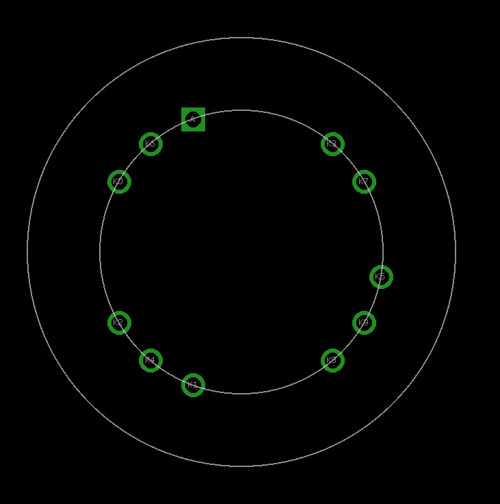
The first step was to build a library containing a schematic symbol and package footprint for the tube. Fortunately, Dalibor has a DXF drawing showing the location of each pin on the tube as well as some advice on creating a do-it-yourself socket using Harwin H3161-01 pin sockets.
The one piece of information missing on the drawing is that the K7 pin is 30 degrees CCW from horizontal but this can be measured / determined from the location of the K7 pin in the DXF drawing. For the pin sockets, he suggests using a 1.95 mm drill when the board will have an ENIG finish and a 2.00 mm drill when the board will have a HAL/HASL finish.
The finished footprint.
I used this information to create a package footprint in Eagle PCB. I’m going to fabricate my boards at OSH Park which uses an ENIG finish so I need to use 1.95 mm drills for the pads. I named my package footprint RZ568M-3161-01-1.95 to remind me that it uses 3161-01 sockets and 1.95 mm drills.
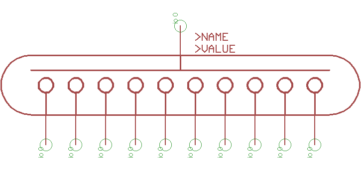
A simple schematic symbol for a 10 digit Nixie tube.
I drew a schematic symbol for a ten-digit Nixie tube then created and connected a device using the schematic symbol and package footprint. I named the finished device RZ568M-3161-01-1.95. If I ever fabricate a board using a HASL finish, I can create an additional footprint and device with 2.00 mm drills and name it RZ568M-3161-01-2.00 to distinguish between the two devices.
Schematic
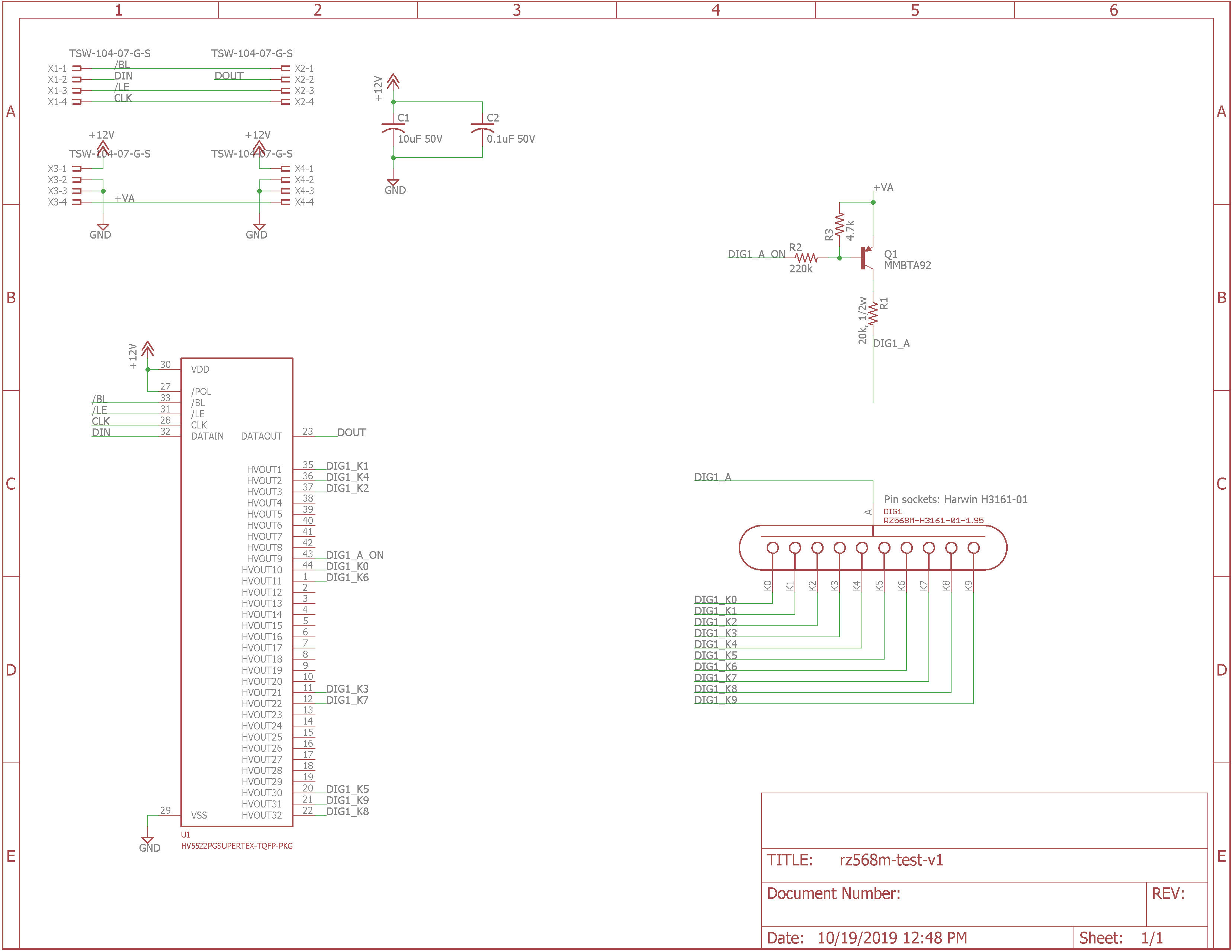
The finished schematic.
Dalibor also has advice on driving the tube on his website. There are links to additional references on there as well. From the information on this page, the tube requires a supply of 170 volts, an 8.2 k current limiting resistor, and some transistors to switch the individual cathode digits on and off.
Instead of using discrete transistors to switch the cathode digits, I’m using a Microchip HV5522-PG 32-channel low-voltage serial to high-voltage parallel converter with open drain outputs. It’s switching transistors are rated to 220 volts which is well above our operating voltage of 170 volts. The only down side to this part is that it requires a 12 volt supply and its serial interface runs at 12 volts rather than the normal 5 or 3.3 volts.
I’m using a PNP transistor to switch the anode voltage on and off. When the HVOUT9 output bit is pulled low, PNP transistor Q1 turns on and voltage is applied to the anode of the tube. This isn’t really necessary but it’s a nice touch to completely shut off the tube when no digits are turned on. Some decoupling capacitors and 0.1″ pitch 0.025″ square post headers finish the schematic.
Board
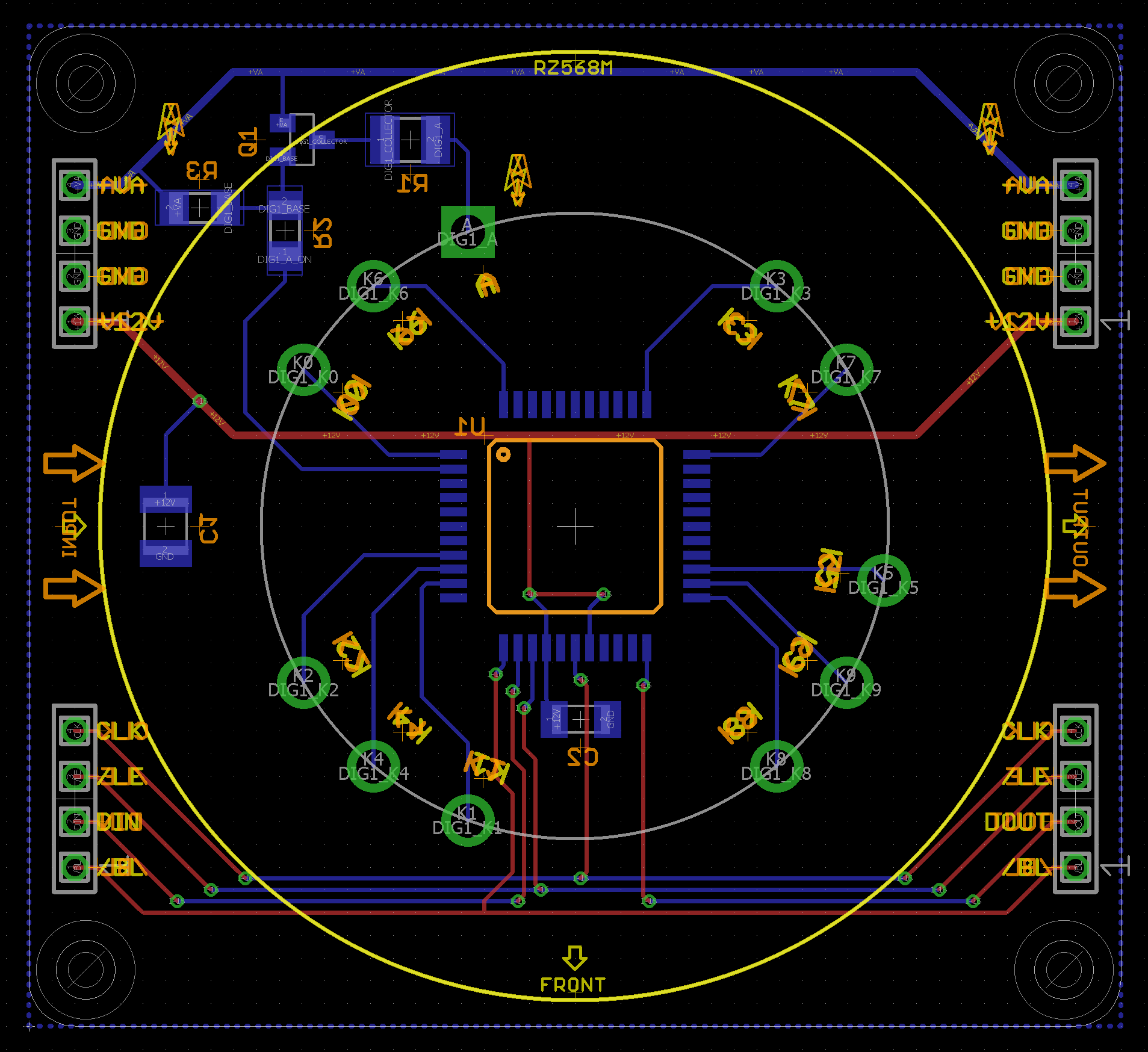
The completed circuit board.
The board design is similar to boards I’ve designed for previous Nixie tube projects. The tube socket goes on top of the board and the remaining components including the HV5522-PG driver go on the bottom of the board. This board will eventually stack on top of a power and control board so the header strips go on the bottom of the board and outside of the tube’s footprint. Some holes for some M3 screws go in the corners of the board.
Assembly

Fabricated socket board.
I had the boards fabricated at OSH Park then assembled them. The Harwin sockets required a bit of force to press them into their holes on the board. Even though they fit tight in the holes, they still need to be soldered in place to make a solid electrical connection. I used the flux and drag technique to solder the HV5522 TQFP to the board and finished soldering the remaining discrete SMD components.
To keep the headers aligned while soldering, I formed a sandwich with two of these boards, all the headers and their sockets, and some 11 mm spacers and M3 screws. Once everything was fixed mechanically, the headers stayed perfectly aligned as I soldered them. Once they were in place, I pulled the boards apart and verified that I did indeed solder the header strips and not any of the header sockets to the board.
Bring Up
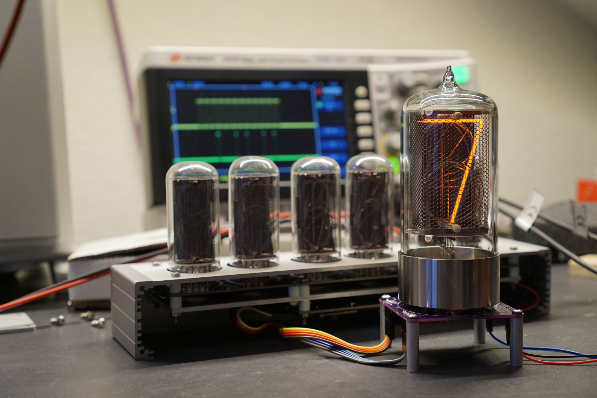
Bring up using the guts of an earlier IN-18 Nixie tube project.
At this point I only had the socket board. I did not have the separate power and controller board. Fortunately the electrical interface on this board is identical to the electrical interface on an earlier IN-18 Nixie tube project I built. I grabbed the IN-18 project, removed enough of the enclosure to access its power and controller board, and connected it to my new socket board using some jumpers.
The HV5522 inside the IN-18 project drives two IN-18 digits. The HV5522 on this board drives a single digit. As a result, the HVOUT connections are completely different between the two projects. I updated the software for the Particle Photon on the IN-18 project’s controller board with the new connections and made a simple test program to cycle through all the digits:
STARTUP(WiFi.selectAntenna(ANT_INTERNAL));
SYSTEM_THREAD(ENABLED);

#define NIXIE_Z568M

#define MKNIXBIT(a) ((unsigned long)(0x1L<<(a-1)))

#ifdef NIXIE_Z568M
#define ANODE  MKNIXBIT(9)    // HVOUT9
#define K0     MKNIXBIT(10)   // HVOUT10
#define K1     MKNIXBIT(1)    // HVOUT1
#define K2     MKNIXBIT(3)    // HVOUT3
#define K3     MKNIXBIT(21)   // HVOUT21
#define K4     MKNIXBIT(2)    // HVOUT2
#define K5     MKNIXBIT(30)   // HVOUT30
#define K6     MKNIXBIT(11)   // HVOUT11
#define K7     MKNIXBIT(22)   // HVOUT22
#define K8     MKNIXBIT(32)   // HVOUT32
#define K9     MKNIXBIT(31)   // HVOUT31
#endif

static const unsigned long DIGDEC[10] = {
    K0, K1, K2, K3, K4, K5, K6, K7, K8, K9
};

int led1 = D7;
int connected = false;
Timer timer (20, tick_50Hz, false);

void setup()
{
    int i;
    unsigned char spiData[12];

    Serial.begin (9600);
    Serial.printf ("\n\r\n\rHello, world!\n\r");

    pinMode (led1, OUTPUT);
    digitalWrite (led1, LOW);

    // disable power supply
    pinMode (A1, OUTPUT);
    digitalWrite (A1, LOW);

    // blank display
    pinMode (A0, OUTPUT);
    digitalWrite (A0, LOW);

    // initialize SPI
    SPI.setClockSpeed (1, MHZ);
    SPI.setBitOrder (MSBFIRST);
    SPI.setDataMode (SPI_MODE1);
    SPI.begin (A2);
    digitalWrite (A2, LOW);

    // turn off all digits
    for (i = 0; i < 12; i++) {
        spiData[i] = 0x00;
    }
    spiSend (12, spiData);

    // enable power supply
    digitalWrite (A1, HIGH);

    // unblank display
    digitalWrite (A0, HIGH);

    // start periodic task to update data displayed on nixie tubes
    timer.start();
}

void loop()
{
    if (!connected) {
        if (Particle.connected ()) {
            connected = true;
            Particle.function ("led", ledToggle);
        }
    }
}

int digit = 0;
int phase = 24;

void tick_50Hz (void)
{
    unsigned long nixieData[3];
    unsigned char spiData[12];

    if (phase == 24) {
        phase = 0;

        nixieData[2] = ANODE | DIGDEC[digit];
        nixieData[1] = ANODE | DIGDEC[digit];
        nixieData[0] = ANODE | DIGDEC[digit];

        spiData[0] = (nixieData[0] >> 24) & 0xff;
        spiData[1] = (nixieData[0] >> 16) & 0xff;
        spiData[2] = (nixieData[0] >>  8) & 0xff;
        spiData[3] = (nixieData[0] >>  0) & 0xff;

        spiData[4] = (nixieData[1] >> 24) & 0xff;
        spiData[5] = (nixieData[1] >> 16) & 0xff;
        spiData[6] = (nixieData[1] >>  8) & 0xff;
        spiData[7] = (nixieData[1] >>  0) & 0xff;

        spiData[8] = (nixieData[2] >> 24) & 0xff;
        spiData[9] = (nixieData[2] >> 16) & 0xff;
        spiData[10] = (nixieData[2] >>  8) & 0xff;
        spiData[11] = (nixieData[2] >>  0) & 0xff;

        spiSend (12, spiData);

        digit++;
        if (digit > 9) {
            digit = 0;
        }
    } else {
        phase++;
    }
}

int ledToggle (String command)
{
    Serial.printf("received command: %s\n\r", command.c_str());

    if (command=="on") {
        digitalWrite(led1,HIGH);
        return 1;
    } else if (command=="off") {
        digitalWrite(led1,LOW);
        return 0;
    } else {
        return -1;
    }
}

int spiSend (int n, unsigned char *d)
{
    digitalWrite (A2, LOW);
    delayMicroseconds (1);

    while (n--) {
        SPI.transfer (*d++);
    }

    delayMicroseconds (1);
    digitalWrite (A2, HIGH);
    delayMicroseconds (1);
    digitalWrite (A2, LOW);
    delayMicroseconds (1);

    return 0;
}
I got a little lazy. This program was a cut and paste job from the IN-18 project so it still drives data to three HV5522 chips instead of just the one I am using on this project. If someone is interested in fixing this in their version of the software, nixieData should be just one word and spiData should be just four bytes to send data to a single HV5522. As you can see in the video at the top of this post, the board works!
Conclusion
That’s the socket and anode and digit cathodes switch board design. In the next post, we’ll design a power and controller board that mounts to the bottom of this board.