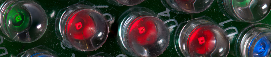
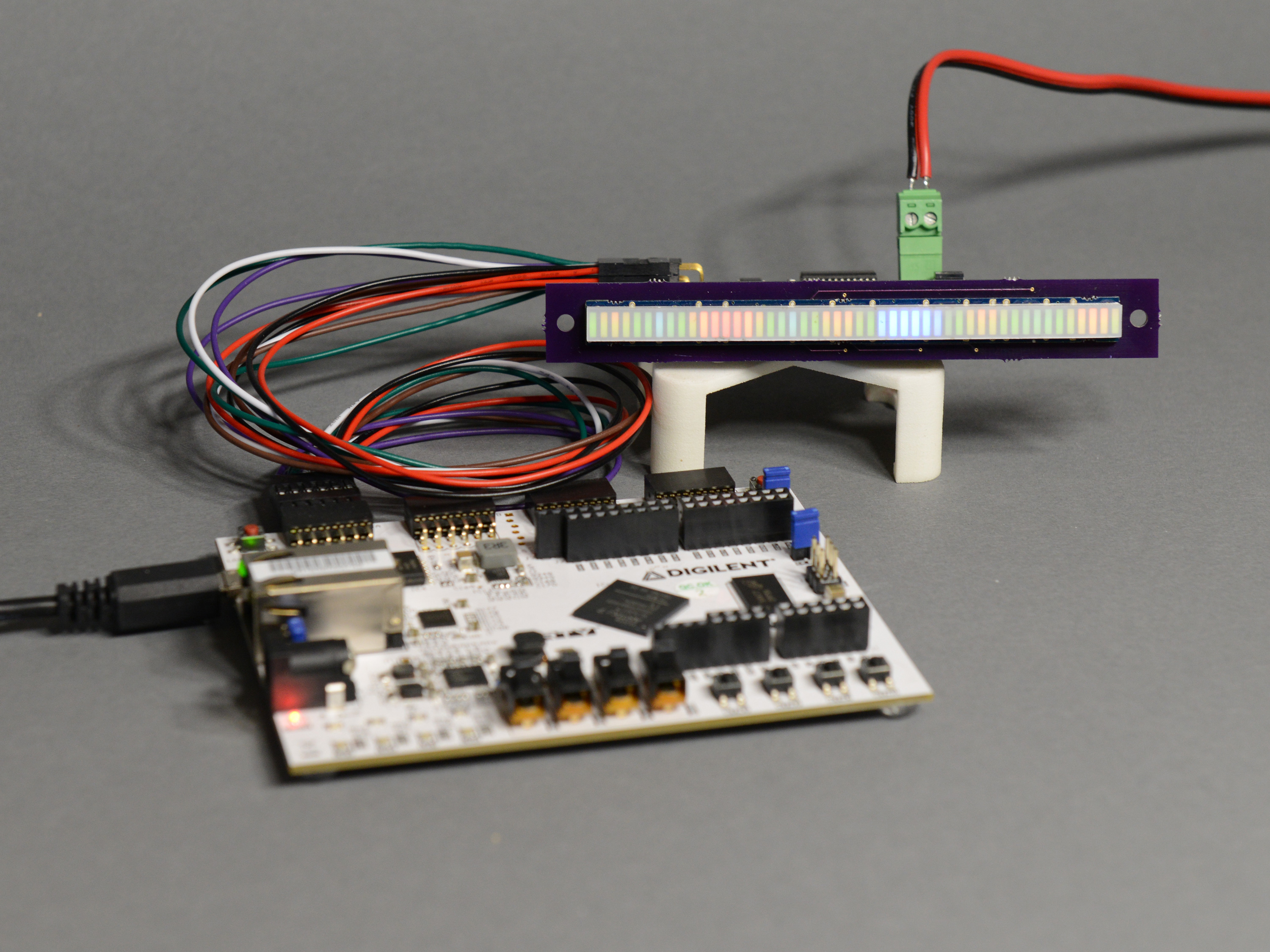
Controlling the RGB bar graph with a Digilent Arty board and my driver and carrier boards. The bar graph is a bit washed out from the lighting used to take the photo.
I recently picked up a 48-segment RGB LED bar graph from SparkFun. The bar graph’s 144 LEDs are arranged in a common-anode matrix of 16 x 9 LEDs. I was hoping to drive the display with something like a Maxim MAX6954 LED display driver. Unfortunately, that display driver is common-cathode and only 16 x 8. A quick Google search found that most display drivers topped out at a 16 x 8 matrix of 128 LEDs—not enough for this application. I quickly came to the realization that I was going to have to build my own display driver.
A few years back, I built some projects using several of the 32 x 32 RGB LED display panels. I decided I’d like to reuse as much of that work as possible and make my 16 x 9 bar graph driver compatible with any hardware or software that could drive one of the 32 x 32 RGB LED panels. The 32 x 32 RGB LED panels have a 4-bit row input, a blanking input, a shift register clock input, a shift register latch input, and two RGB shift register data inputs. I wanted to have a similar interface on my driver board. Now that I knew what the input and outputs of my driver board needed to look like, it was time to start designing.
Block Diagram
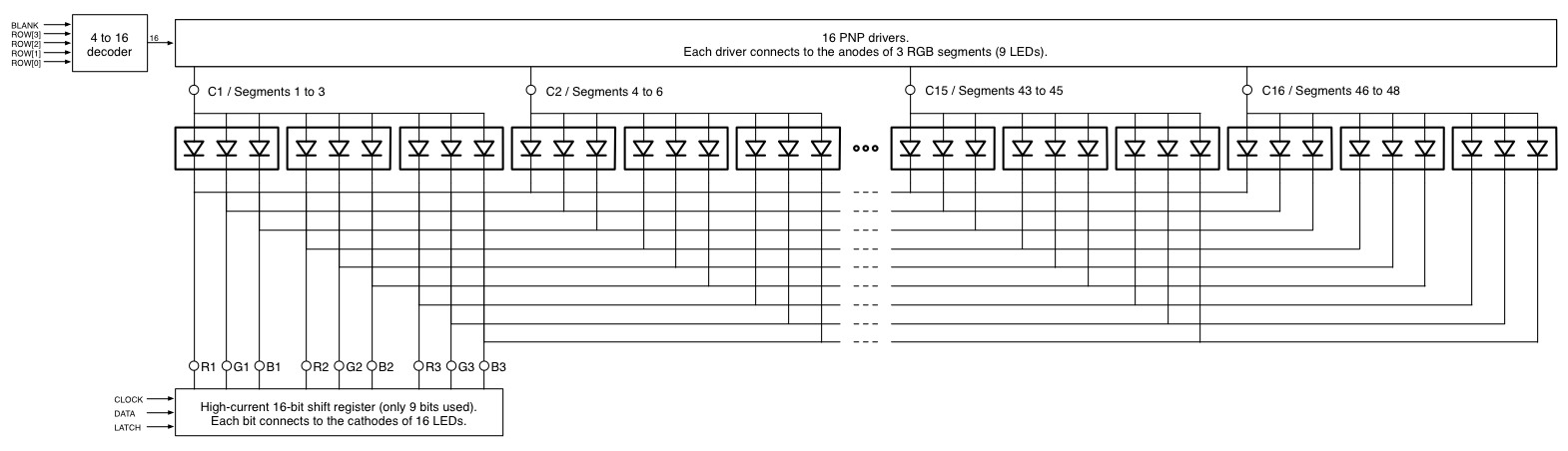
Block diagram of the RGB LED bar graph driver.
The block diagram above shows the basic design of the bar graph and driver circuit. The 144 LEDs in the bar graph are arranged into 16 groups of 3 segments where each segment contains a red, a green, and a blue LED. This is a 16 x 9 matrix of multiplexed LEDs.
To illuminate the LEDs within a group of three segments, apply a voltage to the anodes of the LEDs in that group through one of the sixteen C terminals on the bar graph then connect the cathodes of the LEDs to be turned on to ground through a current limiting resistor using the R, G, and B terminals on the bar graph. To turn on different LEDs, select the next group using the next C terminal and repeat the process. If this is done fast enough, persistence of vision takes over and all the segments can appear to be continuously lit.
High-Side Driver
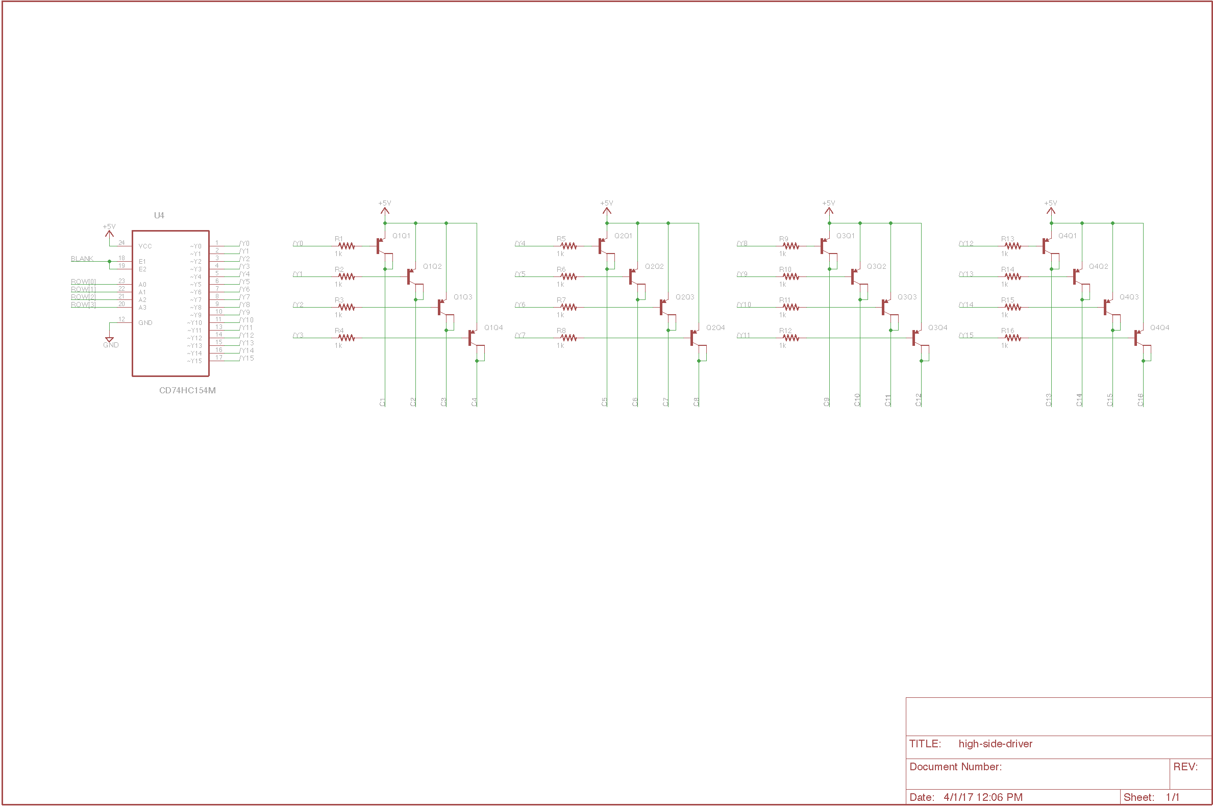
Schematic of the high-side driver for the RGB bar graph display.
To switch the positive supply voltage to the anodes of the LEDs in each group of three segments, I used a 4-to-16 decoder with a disable input and 16 PNP transistors. The disable input serves to blank the display. When the disable input is asserted, all the PNP transistors are turned off and no current can flow through the LEDs thus blanking the display.
When the blanking input is not asserted, the 4-t0-16 decoder will pull low one of its 16 outputs corresponding to the row input. This output is connected to the base of a PNP transistor through a resistor. When the base of the PNP transistor is pulled low, the transistor is turned on and a voltage from the positive supply rail is applied to the anodes of the nine LEDs in that group of three segments.
Low-Side Driver
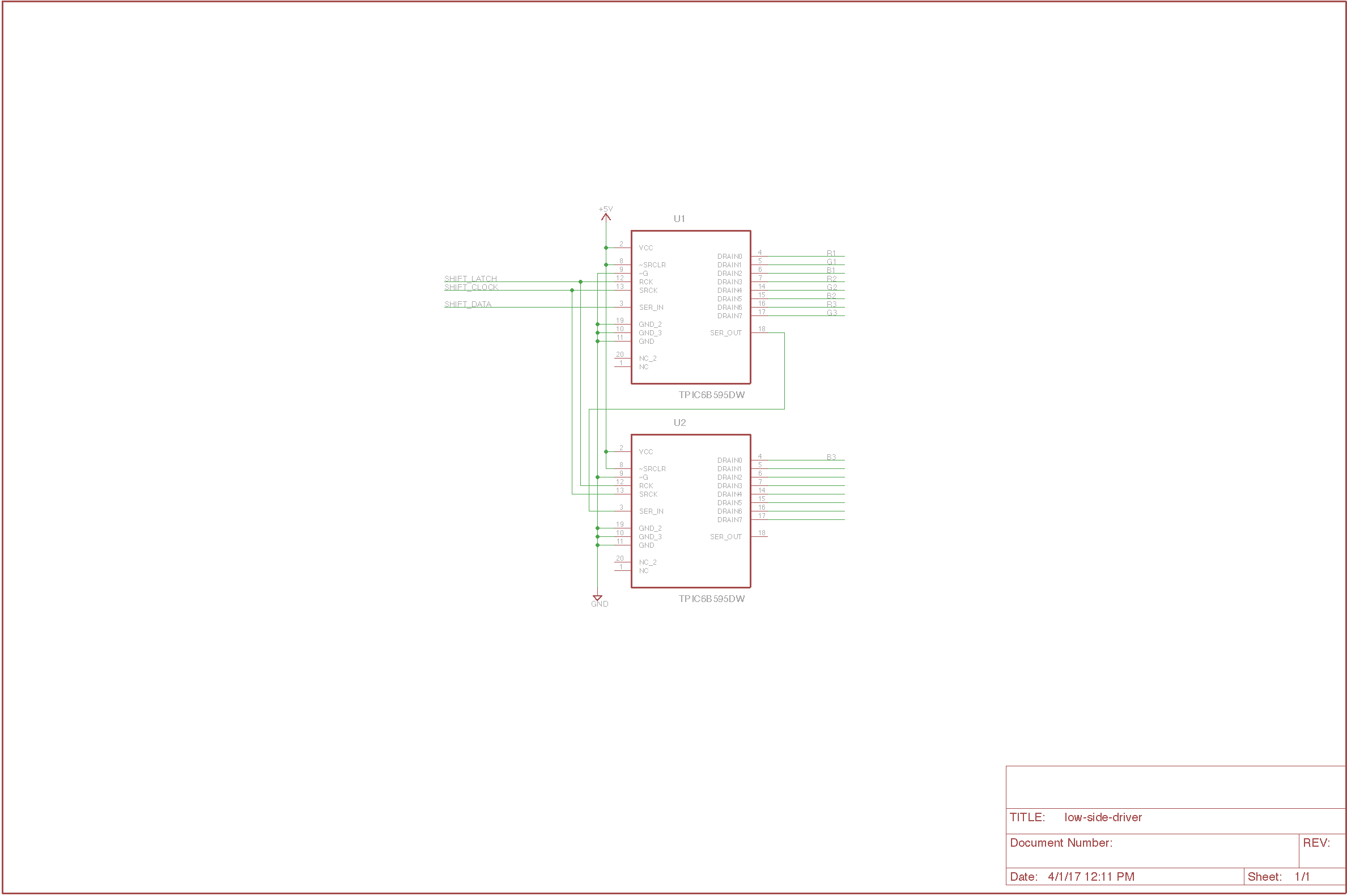
Schematic of the low-side driver for the RGB bar graph display.
Now that a group of three segments has been selected, to turn on individual LEDs within that group, the cathodes of the selected LEDs need to be switched to ground. This is done by shifting and latching bits into the 16-bit shift register. This shift register is a power / driver version of a shift register with open-collector outputs. When a ‘1’ is shifted and latched into a bit position, the shift register’s open-collector output will be connected to the ground rail. When a ‘0’ is shifted and latched into a bit position, the open-collector output will be left open and no current can flow. The 16-bit shift register is built from two 8-bit shift registers cascaded back to back. Only nine bits of the 16-bit shift register’s outputs are used.
Input Connectors and Level-Shifter

Finally, I plan on controlling this board using an FPGA that has 3.3V outputs so I added a Texas Instruments level translator IC to the inputs on the board. The VCCB signal is on the input connectors. If the VCCB signal is connected to +3.3V, the inputs are referenced to +3.3V. If the VCCB signal is connected to +5V, the inputs are referenced to +5V. If the VCCB signal is left unconnected, the driver board won’t function. This design gives the board the flexibility to work with either +3.3V or +5V controllers.
32 x 32 RGB LED Panel Compatibility
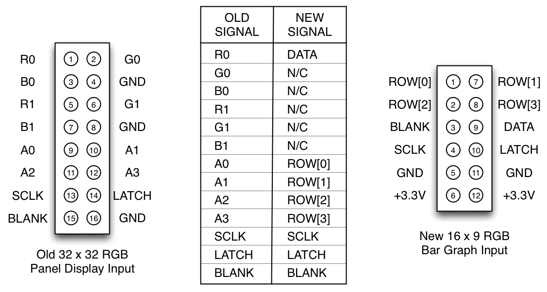
The 32 x 32 RGB panels required a 4-bit row select input, a blanking input , a shift clock input, a shift latch input, and two 3-bit wide RGB shift data inputs. The bar graph driver design has the same inputs except the two 3-bit wide RGB shift data inputs are replaced by a single shift data input that is connected to all three colors of LEDs. With just some software changes, any hardware that can drive a 32 x 32 RGB panel should be able to drive a 16 x 9 RGB bar graph with this design. Use the table in the image above to connect a 32×32 RGB panel controller to the bar graph driver.
Board Design
I decided I wanted my board design to enable mounting of several displays in close proximity to each other on the front panel of an enclosure. This necessitated building two boards that connect at right angles to each other. The first board is a carrier board that holds the bar graph, the current limiting resistors, and a 34-pin header. The second board is the driver board that contains the driver electronics, level translator, and a right-angle header socket to connect to the carrier board.
Carrier Board
Front view of the bar graph carrier board.
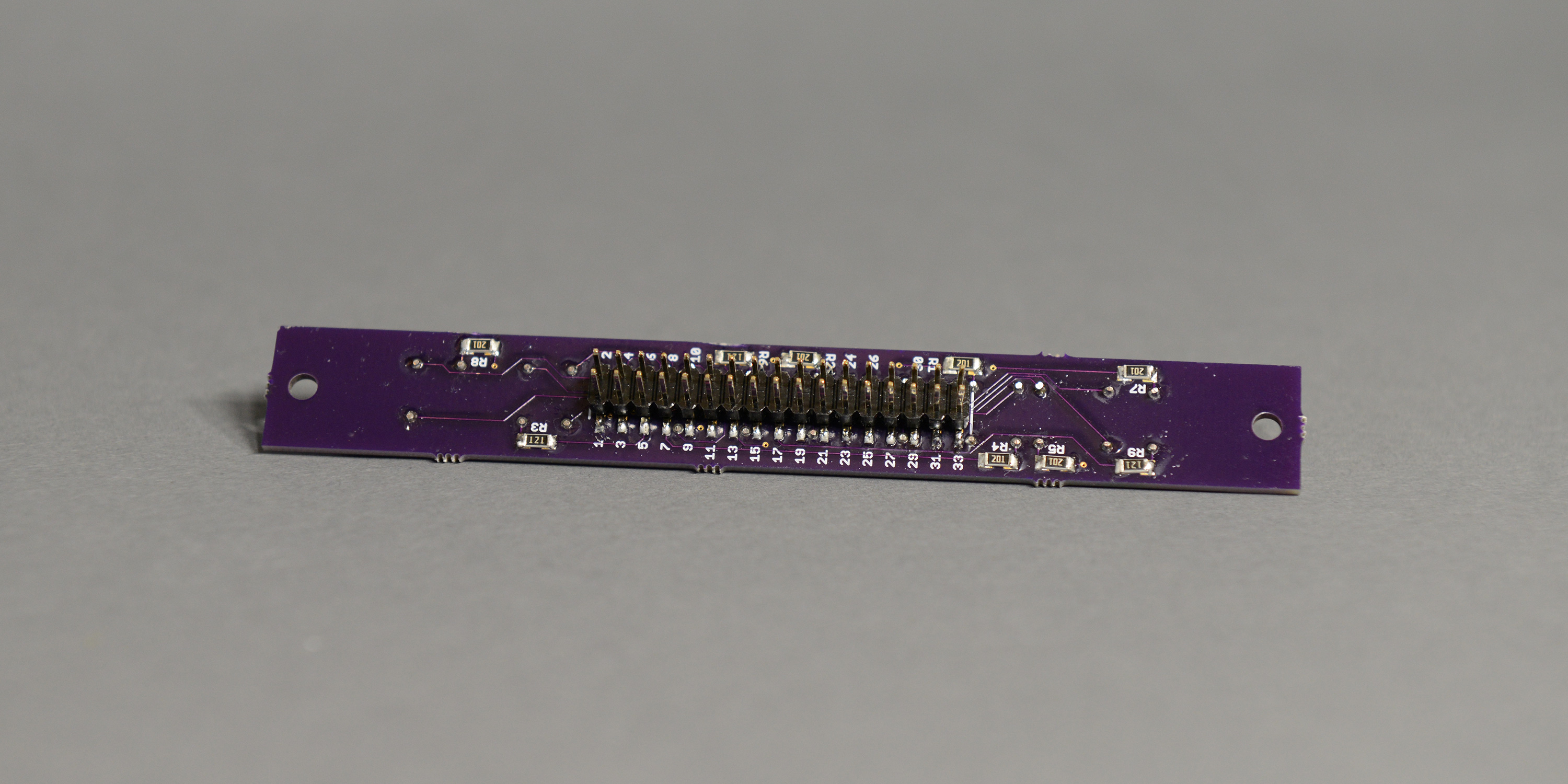
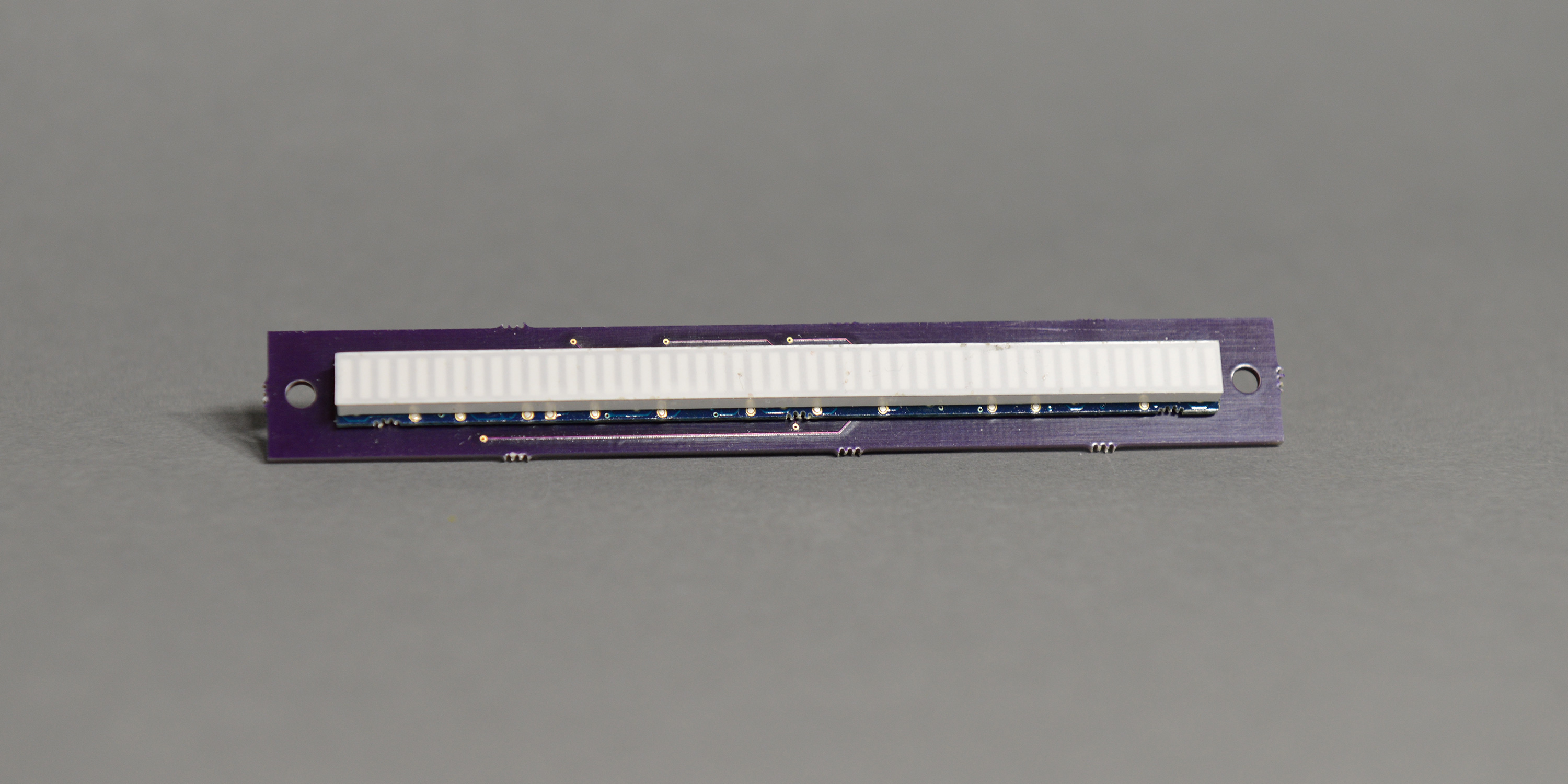
Rear view of the bar graph carrier board.
The carrier board holds the bar graph, current limiting resistors, and a 34-pin connector. The carrier board also has screw holes that can be used to mount the bar graph display to the front panel of an enclosure using some spacers and screws.
Driver Board
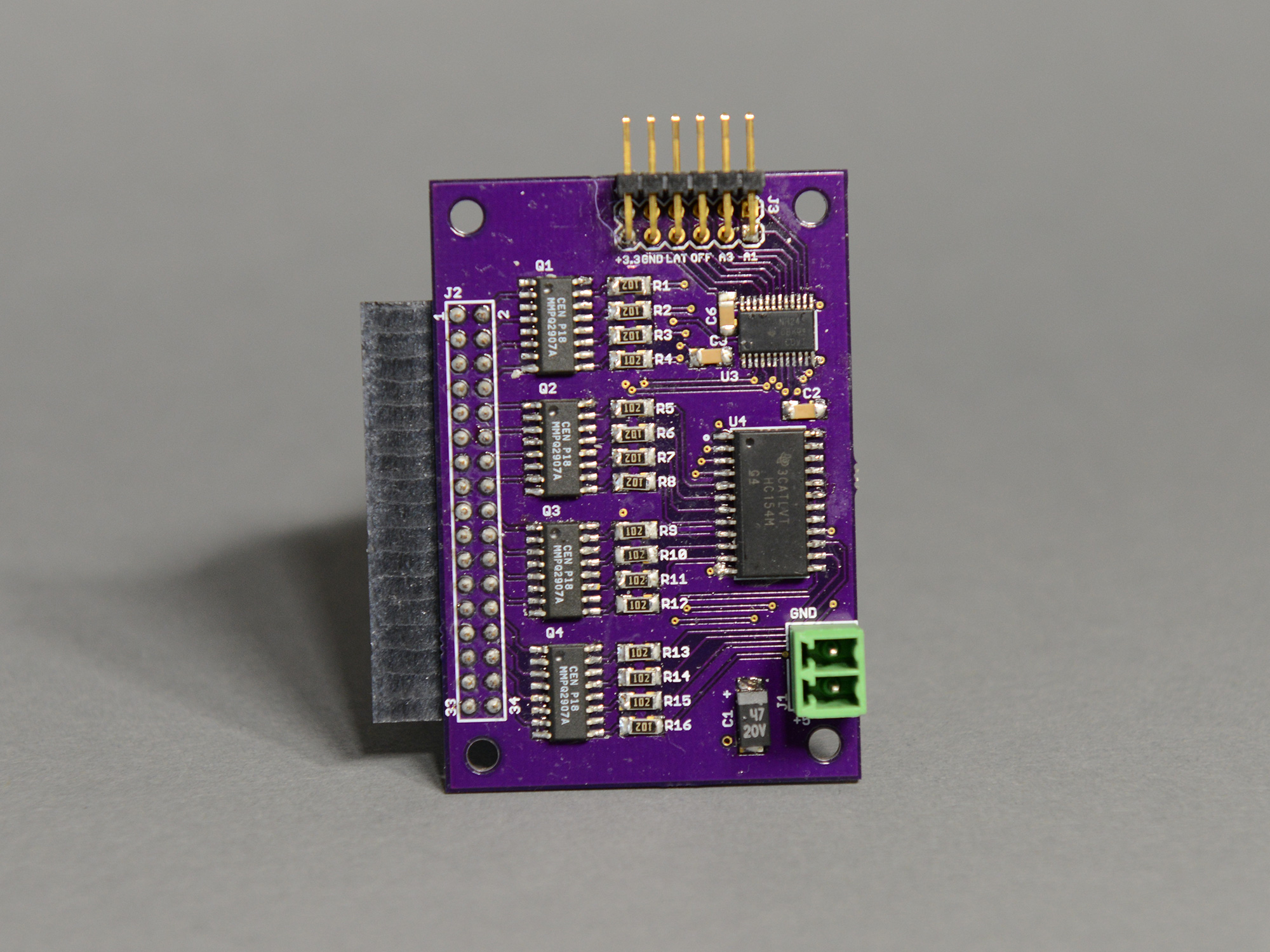
The front side of the bar graph driver board.
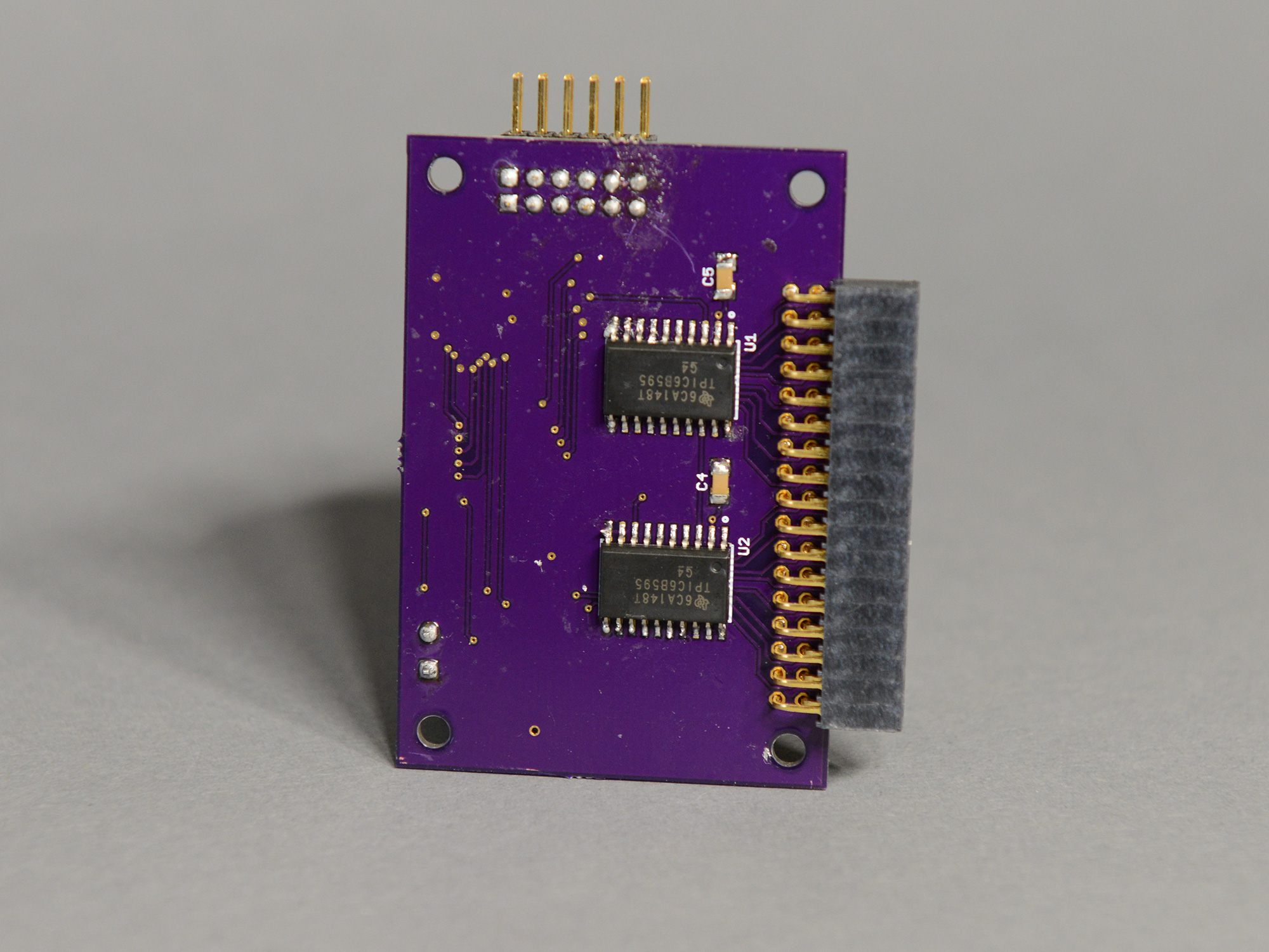
The back side of the bar graph driver board.
The driver board is quite a bit more complicated than the carrier board. It has eight ICs and about twenty passives mounted to both sides of the board. The front side of the board contains the level translator, 4-to-16 decoder, and PNP transistor arrays. The back side of the board has two open-collector power shift registers. Rounding out the driver board design are connectors for the display controller, +5V power, and the carrier board.
Connecting the Two Boards
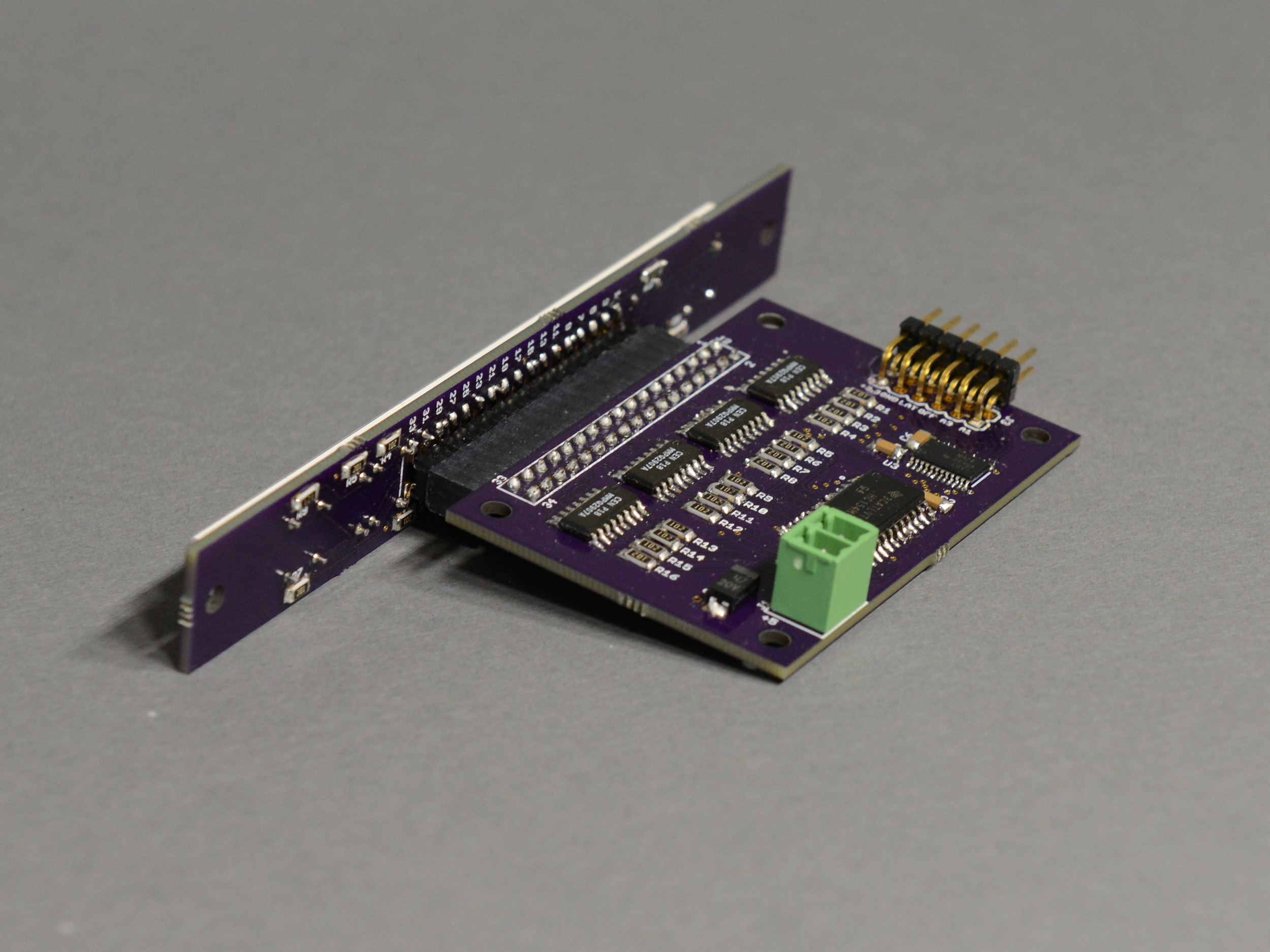
The carrier board mated to the driver board.
The surface mount 34-pin header on the carrier board mates directly with a right-angle 34-pin through-hole header socket mounted to the rear of the driver board. The entire assembly is about 3/4” thick which permits multiple of these assemblies to be placed side-by-side in close proximity to each other on a front panel.
Controlling the Bar Graph Display
Controlling the RGB bar graph with a Digilent Arty board and my driver and carrier boards. The bar graph is a bit washed out from the lighting used to take the photo. I also should have used a right angle power connector on the driver board.
With my driver board, the bar graph display can be controlled with anything that can control one of the 32 x 32 RGB LED panels—Raspberry Pi, BeagleBone Black, Arduino, etc.—with only some small software modifications.
Initially, I controlled the bar graph display using the same BeagleBone Black and Spartan 6 FPGA that I used to control the 6 x 32 x 32 RGB panel video wall. I connected the shift data input pin on the 16 x 9 bar graph driver board to the R0 shift data output pin on the FPGA. Now the red channel used for the top 16 rows of the video wall controlled the RGB data for the bar graph. A few quick software modifications and the display was working.
Once I got some free time, I ported the BBB software and the Spartan 6 FPGA design to a Digilent Arty FPGA board with a Xilinx Artix 7 FPGA. I modified the FPGA RTL to drive a single bar graph display with 24-bit color and replaced the proprietary BBB bus interface with an industry-standard AXI4-Lite interface. The AXI4-Lite interface can connect to a Microblaze CPU soft core in most Xilinx FPGAs or the ARM cores in the Xilinx Zynq series of FPGAs. For the Artix-7 FPGA on the Arty board, I used a Xilinx Microblaze CPU soft core built out of the FPGA’s programmable logic gates. Finally, I ported the Perlin noise software that used to run on the BBB’s CPU to the Microblaze CPU.
Files
The files for making the carrier and driver boards, the RTL for the FPGA, and the software for the Microblaze are available in my Github account. To build the FPGA, you’ll need to package the RTL into a IP, follow the Arty tutorial to build a basic Microblaze design, then import the packaged IP into your Microblaze design.