
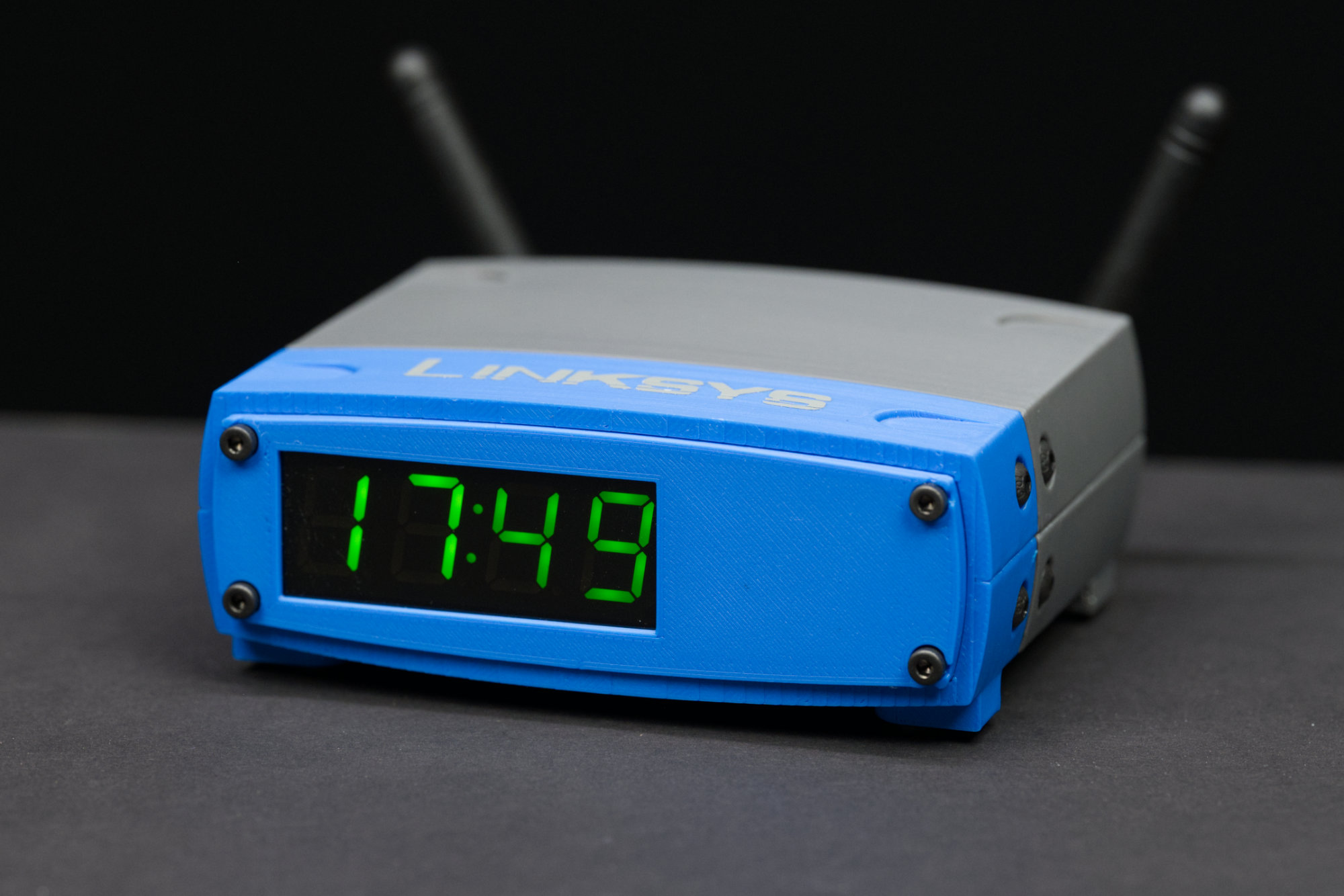
What if Hayes wasn’t the only tech company to build a clock? Here’s my take on a Linksys router clock.
In the early 1980s, Hayes made an external real-time clock styled after their ubiquitous Smartmodem 300. In this project, I explore what it would have looked like if Linksys had built a clock styled after their ubiquitous WRT-54G wireless router from the early 2000s. In the process, I’ll build a Wi-Fi connected, self-setting clock styled like a miniature Linksys WRT-54G wireless router and discover that Linksys products weren’t the first tech products designed to stack.
The Ubiquitous Linksys WRT-54G

The WRT-54G router in the South Park episode Over Logging.
During the early 2000s, Linksys routers, wireless routers, switches, and VoIP adapters were the products to have to run a home network. They were everywhere. If a relative or friend asked what router to get, the answer was always Linksys, and even more specifically, the Linksys WRT-54G wireless router.
The WRT-54G supported IEEE 802.11g wireless, had an upstream WAN port and four downstream LAN ports, and had enough router/firewall features to satisfy those setting up a basic home networking lab. The router was so ubiquitous that South Park featured it in the Over Logging episode that aired on April 16, 2008. In this episode, Kyle fixes the internet for all of Colorado by unplugging a giant version of the router then plugging it back in again.
The Linksys “Stack”
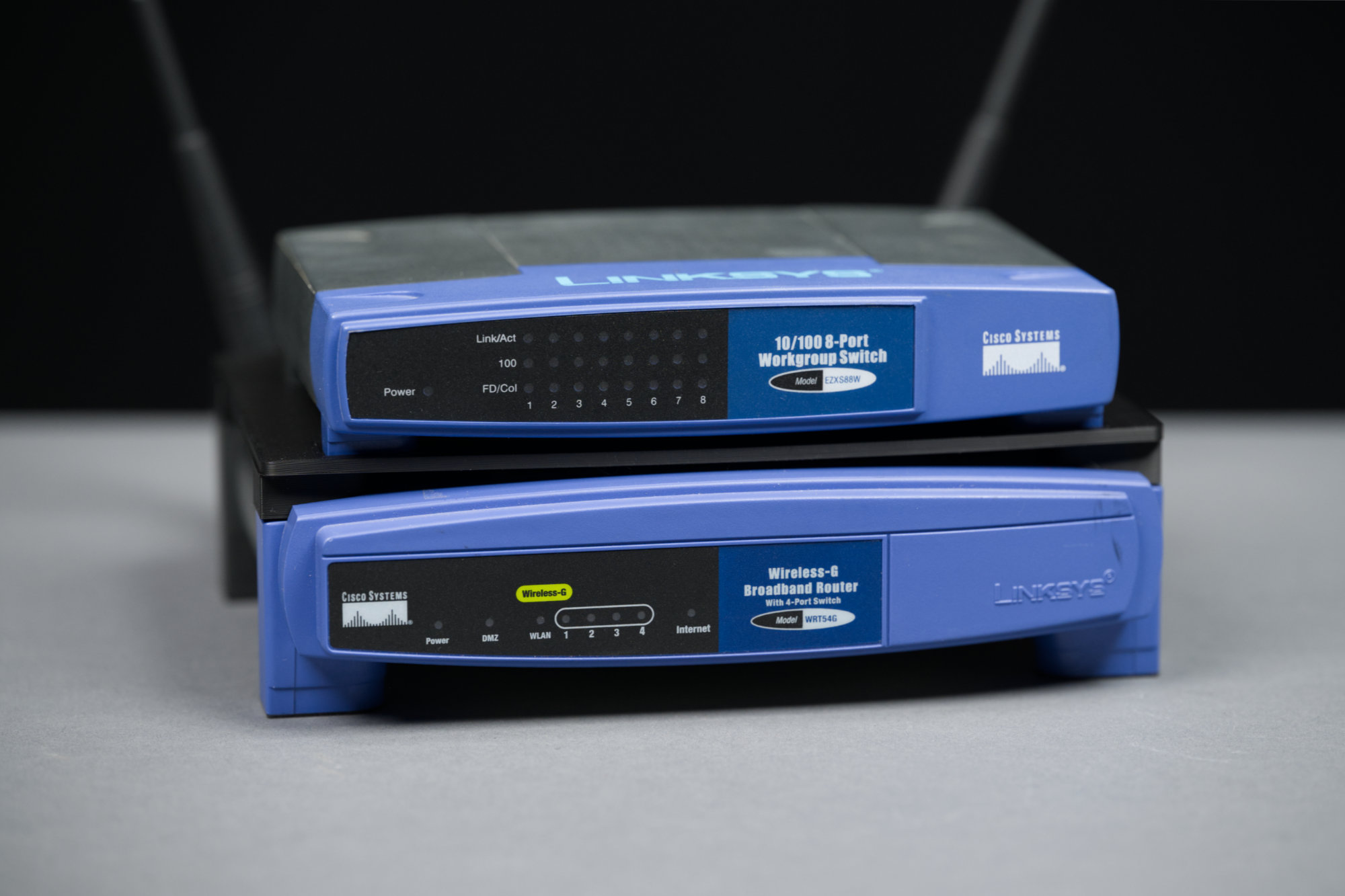
A short stack of Linksys networking products.
The Linksys products were designed to stack. Once you had a WRT-54G wireless router, it was very tempting to stay within the Linksys family for other networking devices like switches, hubs, and VoIP adapters because the devices generally worked well and it was convenient to just add the new device to the stack. For example, the 16-port switch and VoIP adapters had the same footprint as, and stacked directly on top of or underneath, the WRT-54G.
For the smaller devices like the EZXS88W 8-port switch and EZXS55W 5-port switch, Linksys made the SM-01 stacking adapter allowing them to stack on top of the WRT-54G. In the above photo, a EZXS88W EtherFast 10/100 8-port workgroup switch is stacked on top of a WRT-54G using a homemade, 3D-printed stacking adapter similar to the SM-01.
Linksys Wasn’t the First Design to Stack
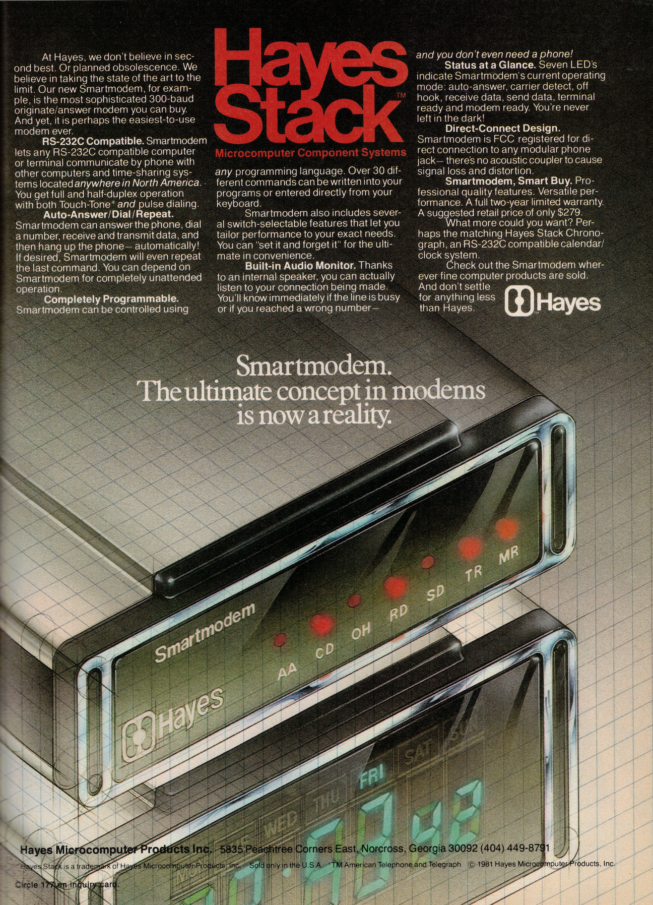
Hayes Stack Smartmodem Advertisement, BYTE Magazine, Volume 6, Number 5, May 1981.
Linksys devices, obviously, weren’t the first tech devices to stack. The credit for first marketing stacking as a feature, however, likely goes to Hayes Microcomputer Products for their Hayes Stack line of products released in the early 1980s. The first product in the series was the Hayes Stack Smartmodem 300 shown in the advertisement above. The modem conveniently stacked under the standard desktop phone of the day.
The Hayes Stack Chronograph
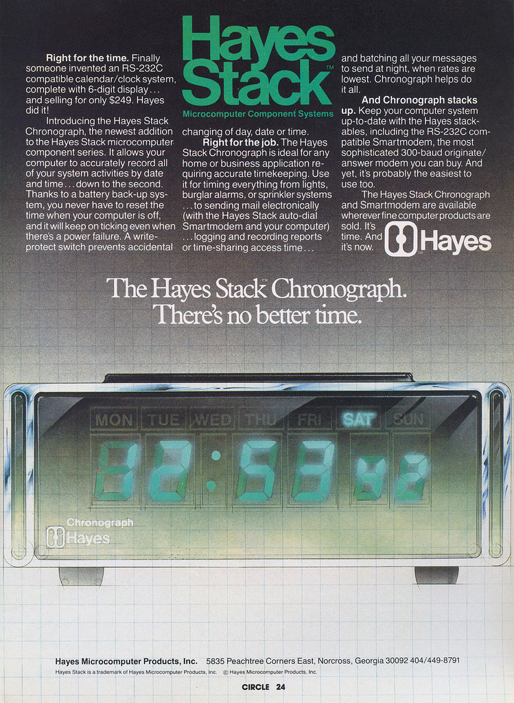
Hayes Stack Chronograph Advertisement.
Only two other Hayes Stack devices were released, a print server and the Hayes Stack Chronograph. An advertisement for the Hayes clock is shown above. This device could stack between the modem and phone and served as an RS-232 connected real-time clock since most, if not all, computers of the day lacked built-in real time clocks. The host computer could send the AT command ATRT to the clock and the clock would respond with the time of day.
The Hayes Stack devices, other than the modem, proved rather unsuccessful overall though and stack was eventually dropped from their marketing. From Wikipedia:
Hayes originally had big plans for the form factor, referring to it as the Hayes Stack and intending to release a range of products that could be stacked beside the computer. In the end, only two non-modem devices were added to the line. The Hayes Stack Chronograph, an external real-time clock and the Transet 1000, a printer buffer and primitive email box. Both of these items’ sales were apparently dismal. Early advertising referred to the Smartmodem as the “Hayes Stack Smartmodem”, but this naming convention was dropped a short time later.
The Router Clock Is Born
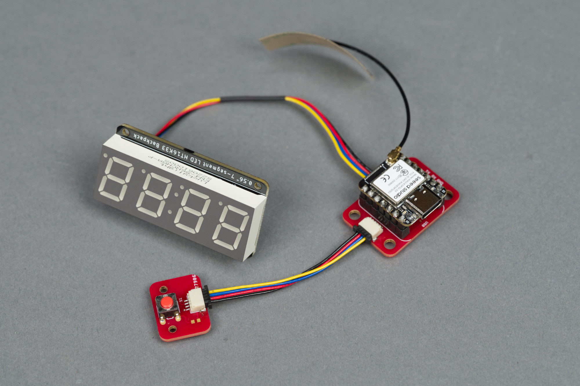
These are all the parts that are required for a Wi-Fi connected, NTP-enabled digital clock.
About the time that I was toying with the idea of designing a Linksys-like enclosure that could be 3D-printed, Lee Hutchinson on Ars Technica wrote an article about an overly-engineered clock he built. I quickly prototyped a smaller, less-complicated version of his clock using components I had around the house. Inspired by his clock, my early prototype, and the Hayes Chronograph, I decided a clock would be the perfect vehicle to try to make my own Linksys-like enclosure.
Designing a Linksys-Like, 3D-Printed Enclosure
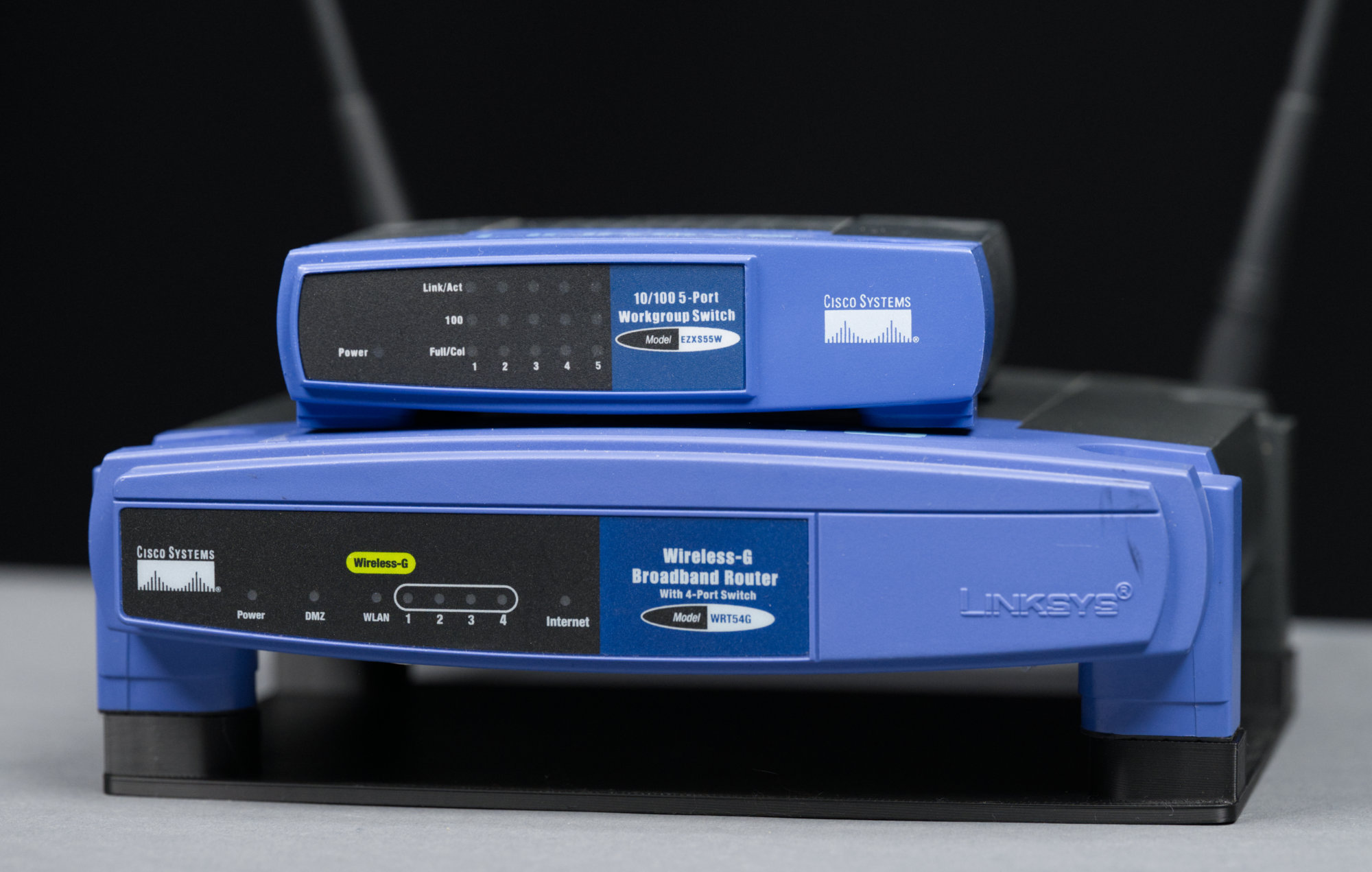
The WRT-54G and a much smaller 5-port Ethernet switch.
Linksys had a smaller enclosure design they used for the EZXS55W 5-port 10/100 workgroup switch. It’s a smaller version of the wireless router design with less prominent legs. It will stack with itself but not with the larger components without an adapter. I decided to make my clock roughly the size of the 5-port hub, shown above, to minimize the material used, minimize the print time, and to make it a cuter, smaller version of the WRT-54G.
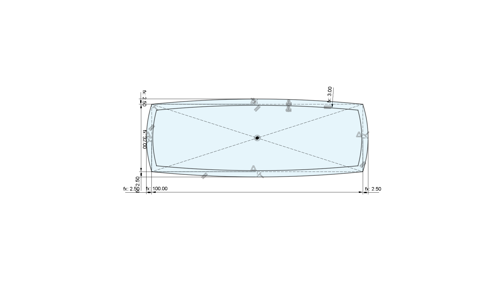
Sketch used to establish the basic shape of the enclosure.
The basic router shape is relatively simple: a rectangle with bulging sides. In this case, the base dimensions are 100 mm wide by 32 mm tall with a bulge of 2.5 mm in each direction. Since the front and rear shells are going to overlap a bit, I went with a shell thickness of 3 mm to give me more room to make the overlap and gap where the shells meet. This is the inset outline in the image above. The design is fully parameterized so I can adjust the width, height, bulge, and shell thickness in Fusion’s modify parameters dialog.
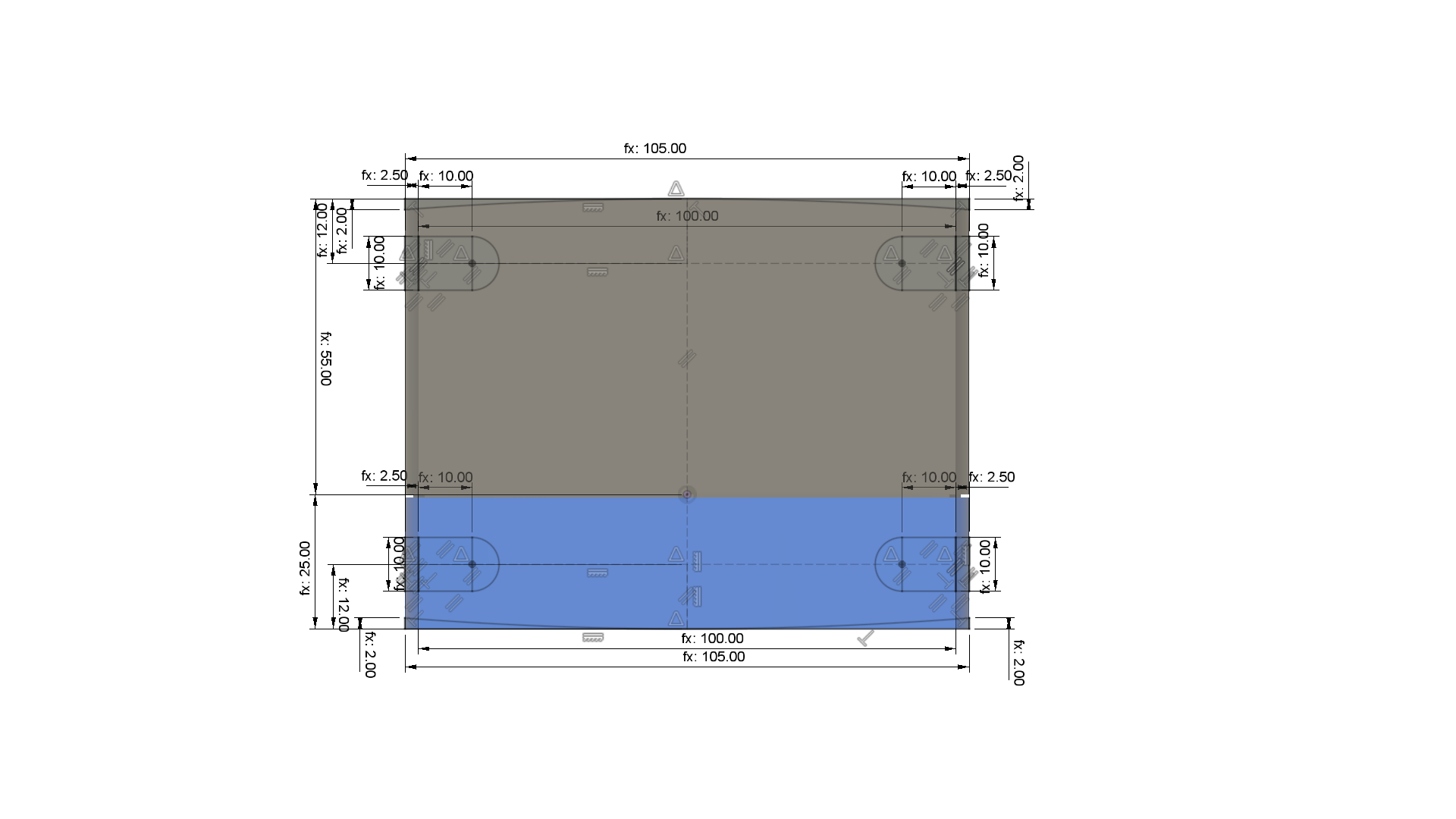
Sketch used to create the feet, stacking indents, and curve the front and rear of the enclosure.
The front and rear of the router are also bulged. To form this bulge, I constructed arcs along the front and back shells and used the extrude tool to cut the bulges into the bodies. The feet and indents are constructed from a rectangle and a circle. The feet are constructed from a joined body extruded down from the bottom of the enclosure. The indents to make this design stackable with itself are cut and extruded up from the top of the enclosure.
Again, everything in the design is parameterized so that the bulge depth and the location and size of the feet can be adjusted in Fusion’s modify parameters dialog. I did not intend for this enclosure to stack with the 5-port switch, but with some adjustments to the parameters, it should be able to be made stackable, he said foreshadowingly.
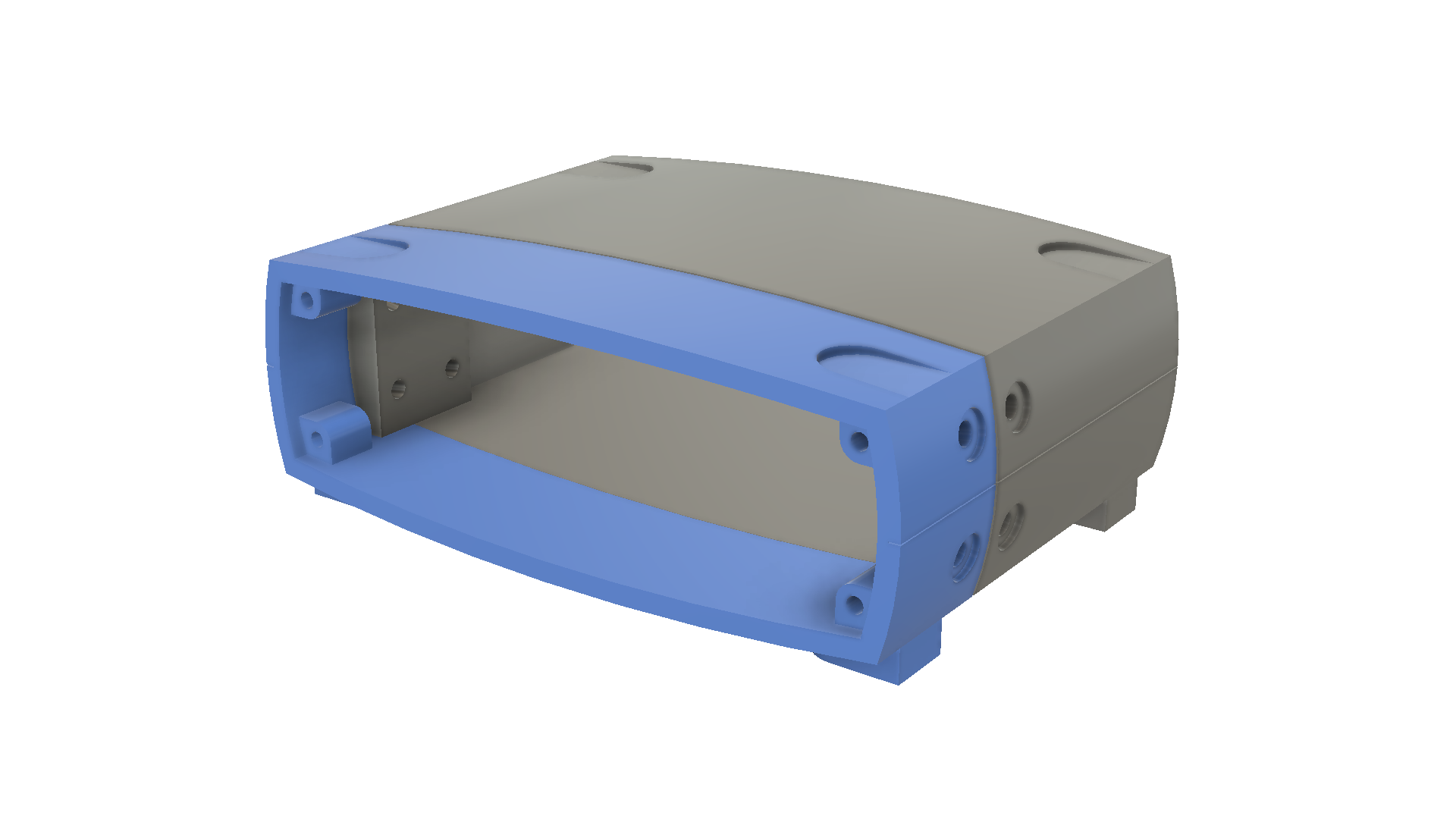
The completed front and rear housing assemblies.
A render of the completed front and rear shells is shown above. I added an overlap where the gray and blue pieces come together, some extrusions to support the front and rear panels and secure them with M3 screws, and a method to join the two halves together.
The halves of the real routers supposedly snap together. I have not taken one apart to see. Instead of snapping together, the two halves of my enclosure screw together using separately printed joiners. The screw heads are parallel to planes tangent to the surface of the shells so all the screws thread into the joiner at an angle toward the center of the enclosure.
While designing the enclosure was relatively simple, the biggest problem with a Linksys-like enclosure is that every surface is curved and thus it is not easy to find a flat surface to orientate down to the print bed. Any curved surface pointed toward the print bed requires support material and will have artifacts after removing the support material. Any curved surface pointed away from the bed has distinct layers visible.
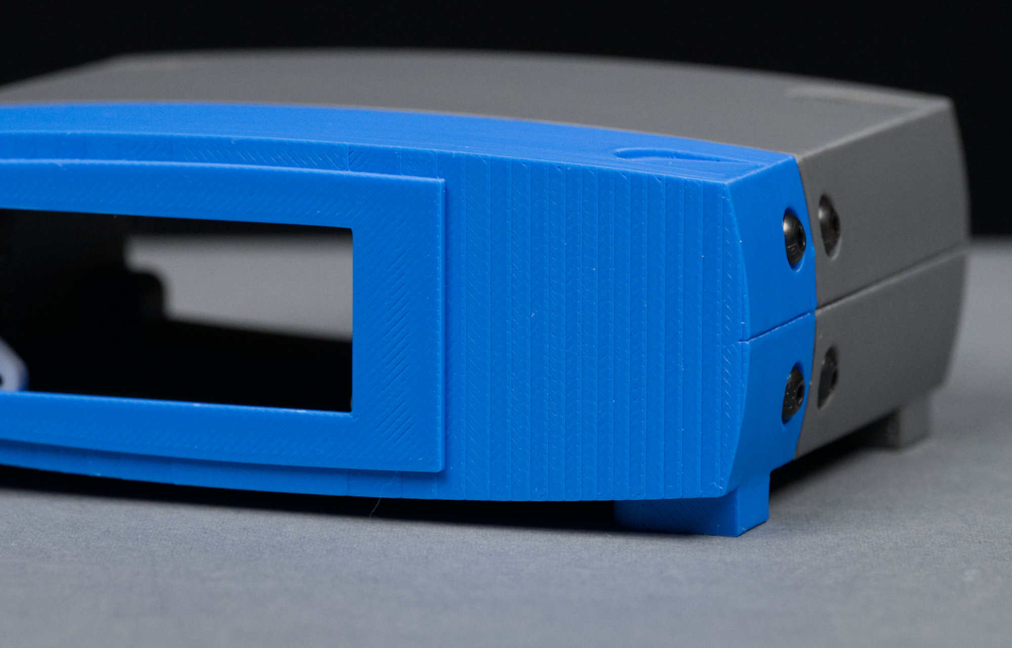
Distinct layers can be seen in the curved face when the single-piece front design is printed face up.
The photo above shows what happened when I tried to make the front part of the enclosure a single-piece unit. This print was filled with support material that was difficult to remove. More troublesome, it has extremely obvious and distinct layers making up the curved part of the front panel. These are artifacts of how FDM 3D printers use layers to build up a print.
After this experience, I decided to make the front and rear panels flat and separate from the main housing bodies. This also meant I could print a single-housing then swap the front panels as the clock design evolved or swap the panels to repurpose an already-printed housing for an entirely different project.
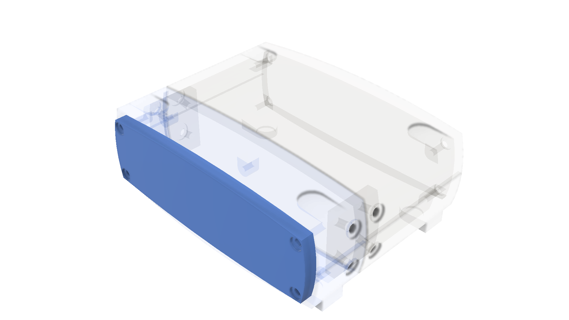
The blank front panel. It extends from the enclosure.
The photo above shows the completed, blank front panel. It extends a bit from the front shell just like on the real router and switch. I’m using 2.5 mm socket head cap screws in a slight recess to secure the front panel to the front shell.
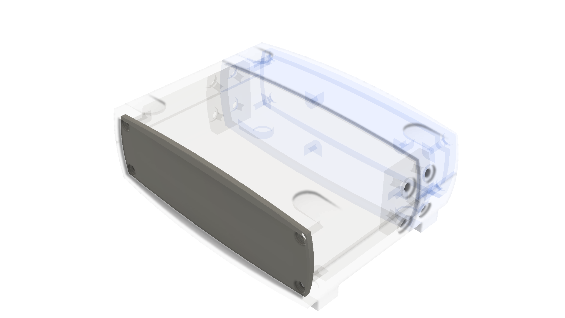
The blank rear panel. It is inset into the enclosure.
The photo above shows the completed, blank rear panel. It is recessed a bit into the rear shell just like on the real router and switch. I’m using 2.5 mm socket head cap screws in a slight recess to secure the rear panel to the rear shell.
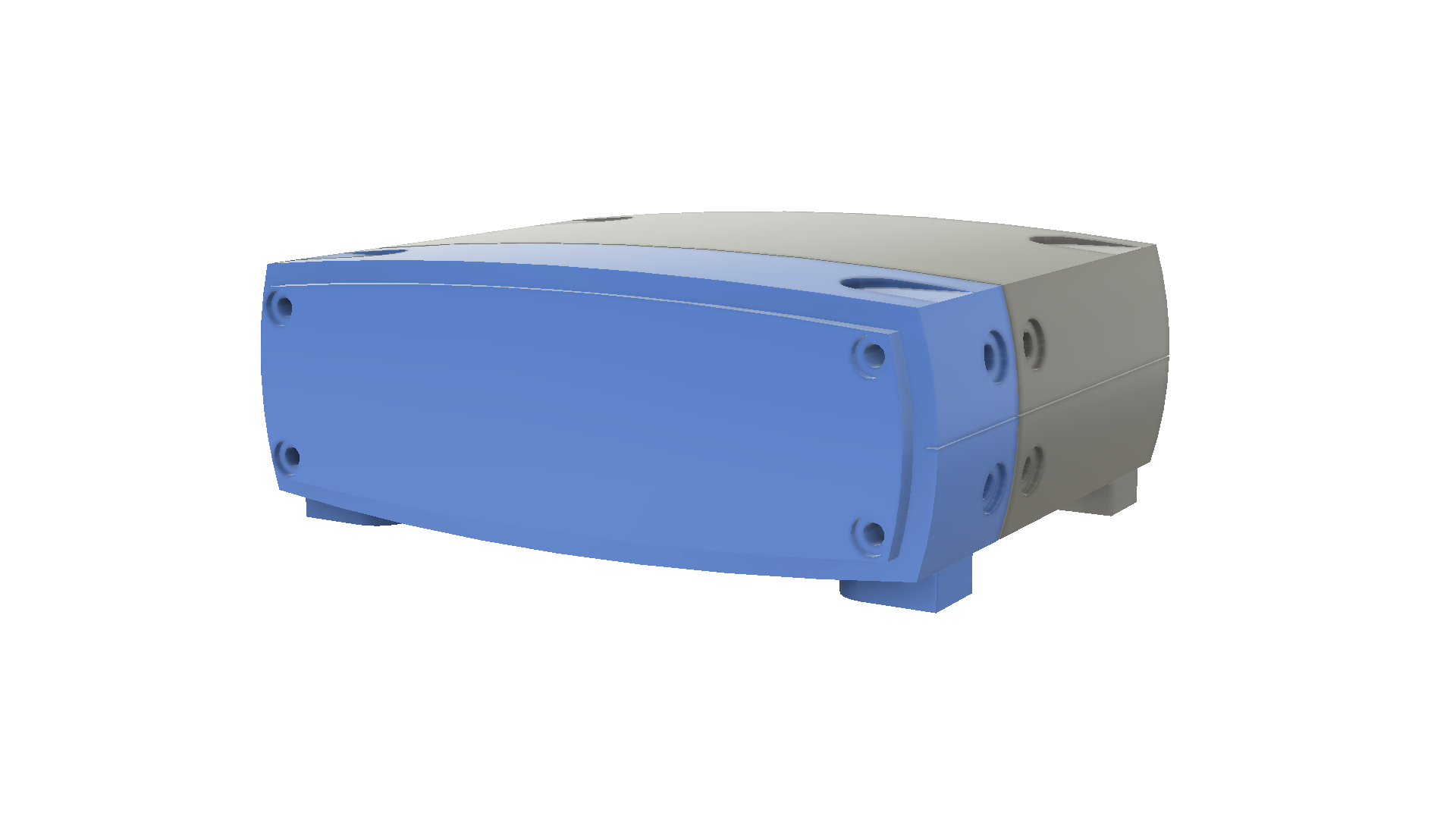
The completed enclosure with blank panels.
The render above shows the completed enclosure design with the blank panels. While distinct layer artifacts will still be visible on this design, they will be limited to a 3 mm wide band surrounding the bolt-on front and rear panels. As such, they are much less noticeable than when the entire front panel is curved.
The Button and ESP32-S3 Carrier Boards
My router clock uses a Seeed Studio XIAO ESP32-S3 development board to control everything. It has Wi-Fi and a connection for an external antenna and is programmable using the Arduino development environment. I built a small carrier board to mount the XIAO board on the rear panel of the enclosure and add a +5V QWIIC interface and a connector for a button to the XIAO board. I also built a small board with a single button on it. Let’s look at the button board first.
The Button Board
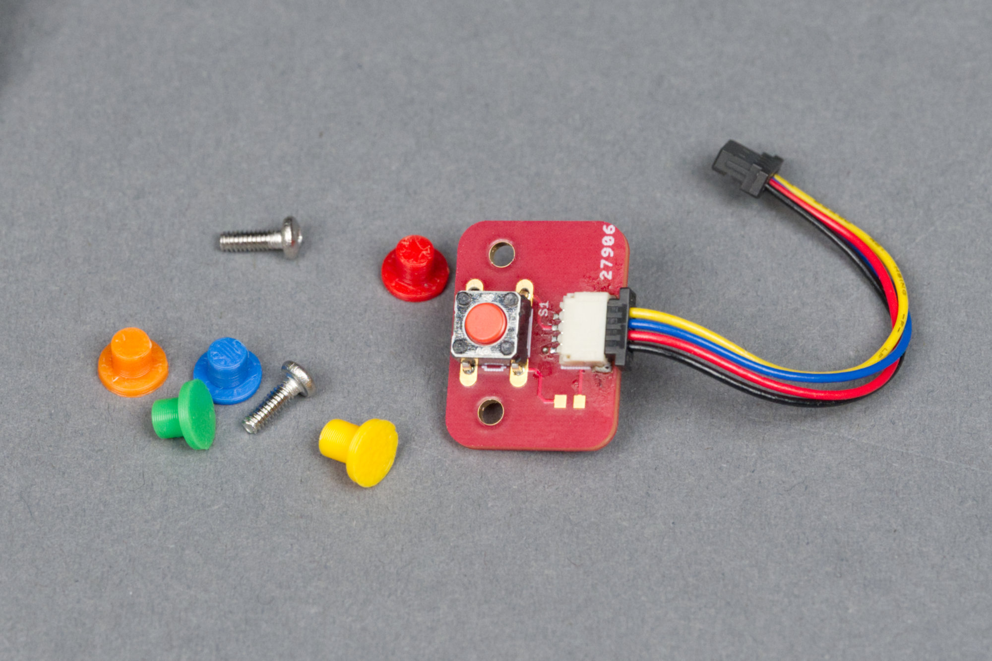
The assembled button board and several 3D-printed colored plungers.
The clock needs a button to force the Wi-Fi into access point mode so that the Wi-Fi SSID and password, time server, and timezone can be set with a mobile phone or laptop. The button is on its own circuit board and connects to the carrier board using a QWIIC cable even though the button is not IIC and uses a GPIO pin instead.
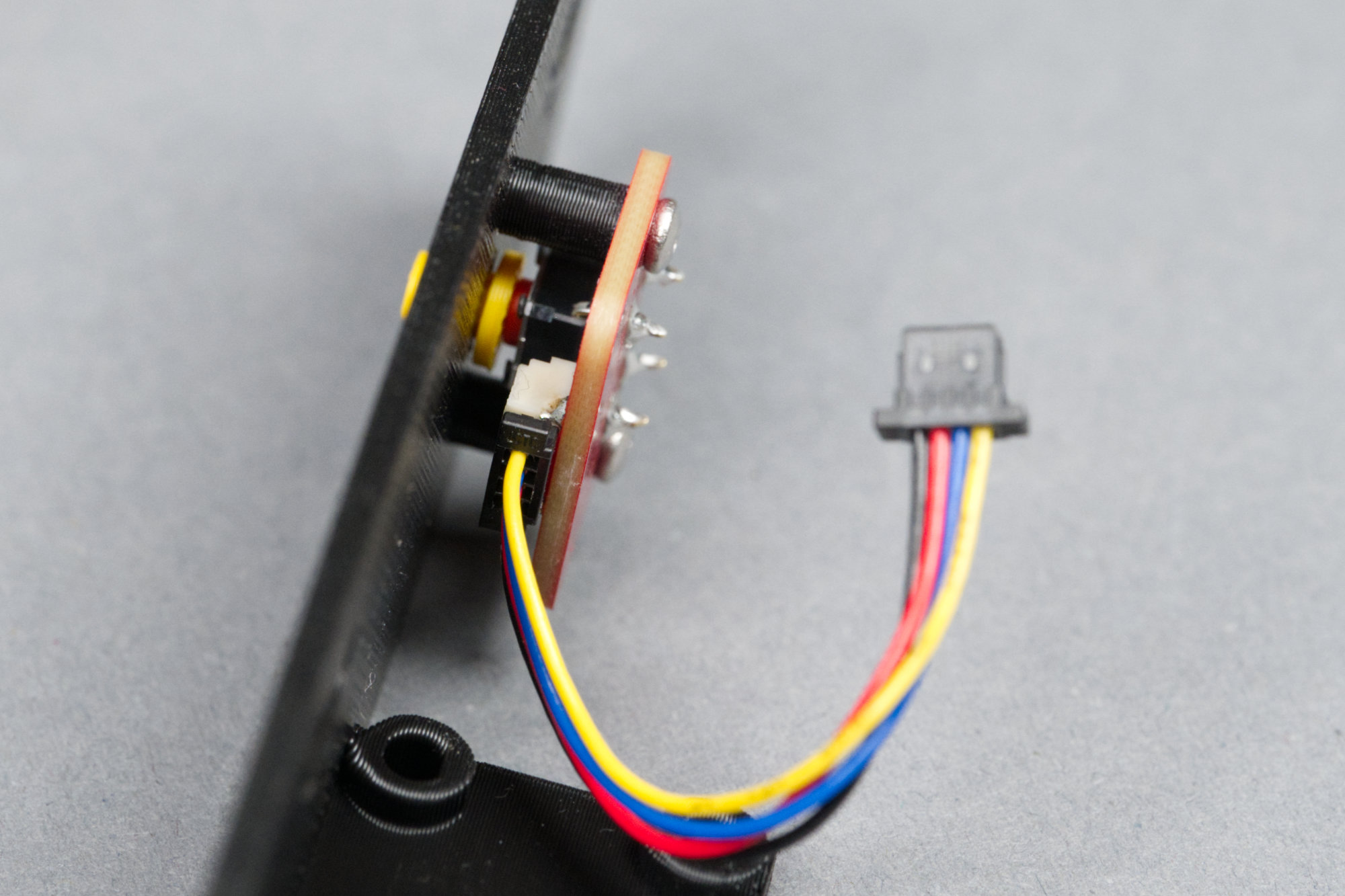
The button and plunger on the rear panel of the enclosure.
The button mounts to the rear of the rear panel using 2 M2 x 6 mm screws. A 3D-printed plunger, shown in yellow above, extends through the rear panel to permit the tactile switch to be pushed by the user. If you have a favorite panel mount button, that could be used instead of the button board and plunger.
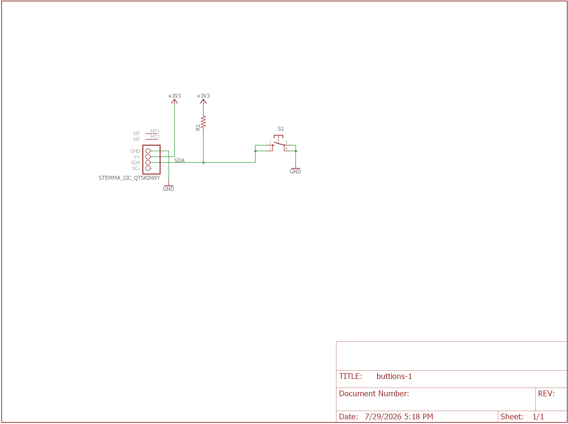
Button board schematic.
The schematic is super simple and, as long as the micro supports inputs with internal pullups, the resistor is optional.
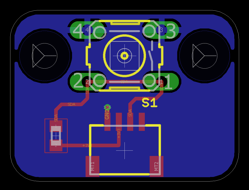
The button board PCB layout.
The layout of the button board is shown above.
The ESP32-S3 Carrier Board
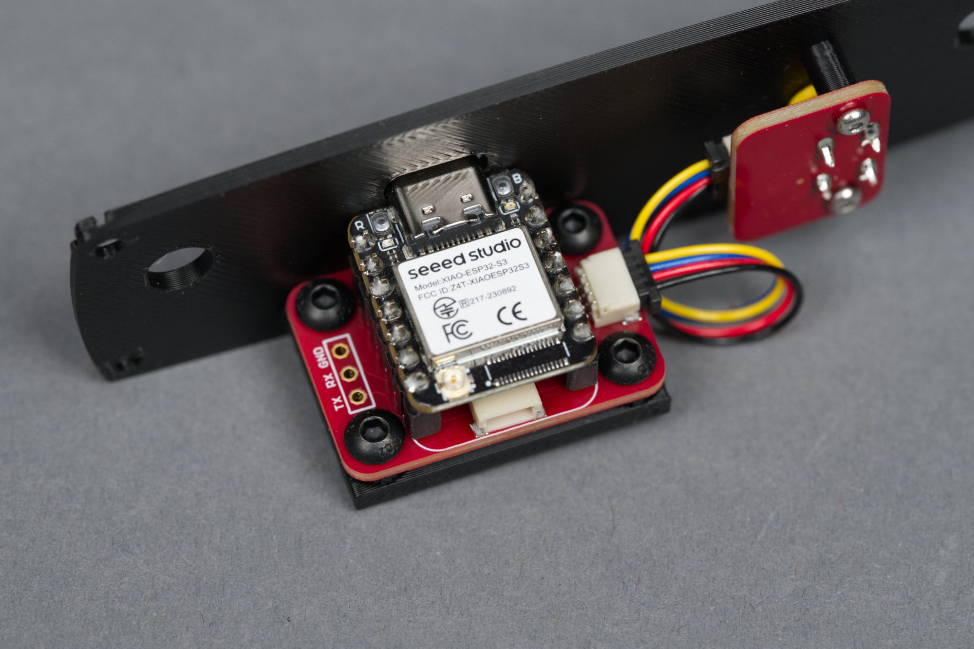
This board holds the XIAO ESP32-S3 dev board in place and converts the QWIIC interface to +5V power and logic.
The carrier board’s primary purposes are to mount the XIAO board with its USB C connector externally accessible and to interface to the four-digit, seven-segment clock display’s IIC interface and the AP mode button.
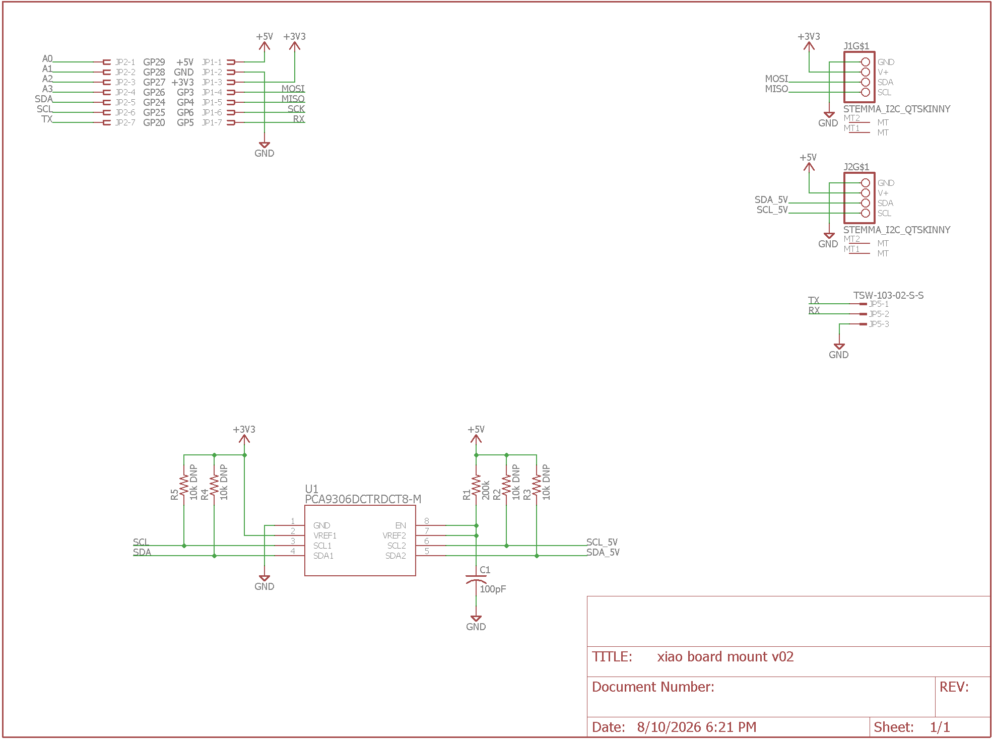
The XIAO ESP32-S3 carrier board schematic.
The clock display’s IIC backpack is a 5 V device. The XIAO is a 3.3 V device. The clock power must be supplied by the XIAO’s 5 V pin and a level shifter is required to convert the XIAO’s 3.3 V IIC interface to match the display backpack’s 5 V interface. This is done with the PCA9306 IIC level shifter in the schematic above. The button has its own QUICC connector but the connector is only connected to 3.3 V, ground, and a few GPIO pins.
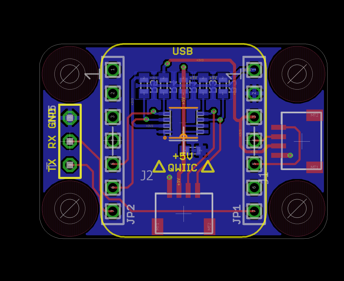
The XIAO ESP32-S3 carrier board layout.
The carrier board’s layout is shown in the image above. The bottom QWIIC connector is the 5 V interface to the display. The right QWIIC connector is for the button. The TX/RX/GND header is not used in the current design but is available for additional I/O or interfacing.
The Front Window Acrylic
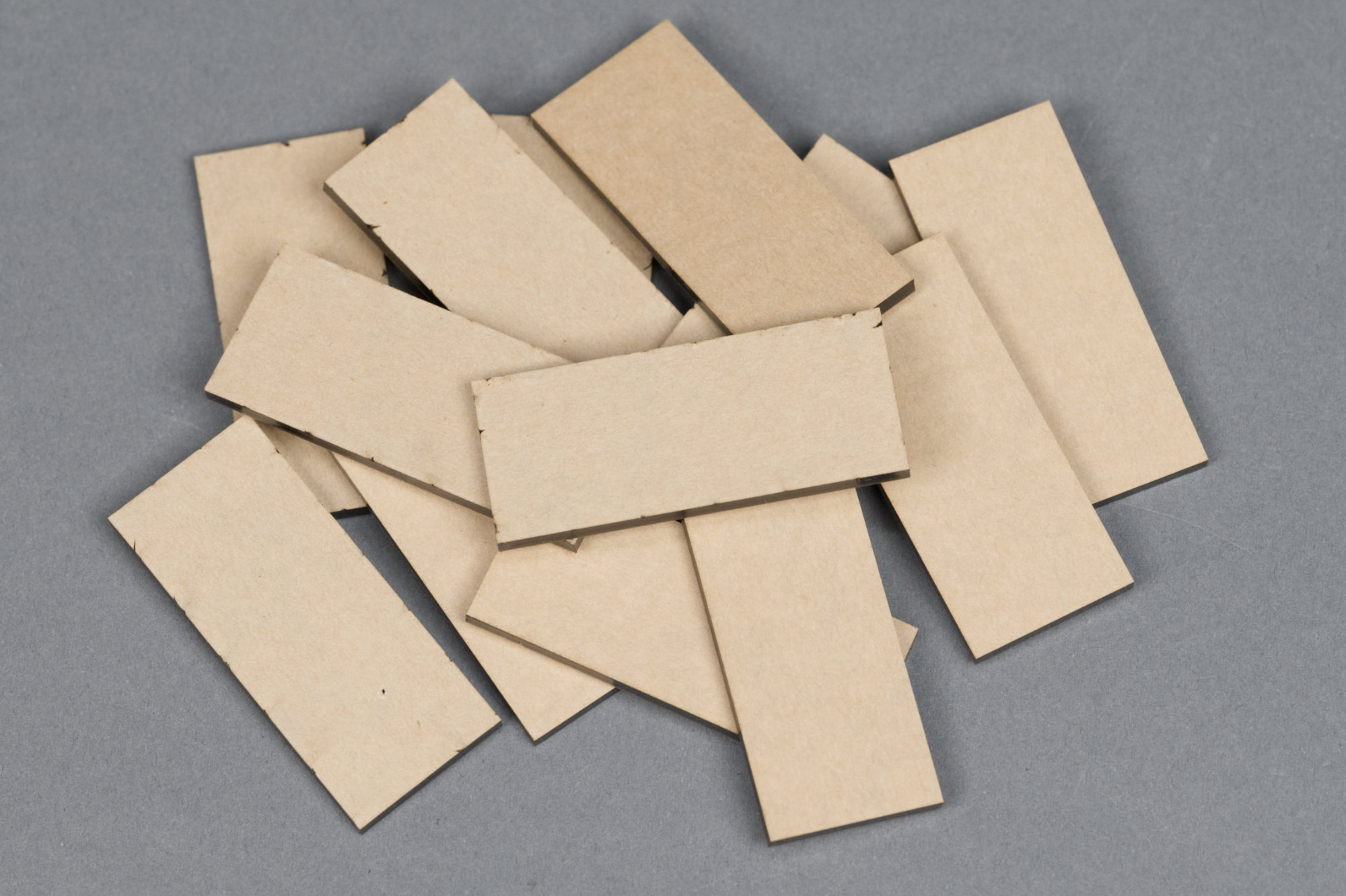
13 of the 14 acrylic windows I ordered.
The front window of the clock uses a piece of dark gray transparent acrylic to give the clock a finished look. The LCD and front panel opening are 50.4 x 19.4 mm. Inside the front panel is a 54.40 x 23.40 x 2 mm pocket to hold the acrylic. The acrylic is 54 x 23 x 3 mm so that it fits easily inside the pocket. There’s a 1 mm gap between the pocket and the display so the 3 mm acrylic fits perfectly. The windows were cut at SendCutSend using their Dark Gray Acrylic #7074, 0.118″ (3 mm) material.
Adding the Button, Display, and Micro to the Model
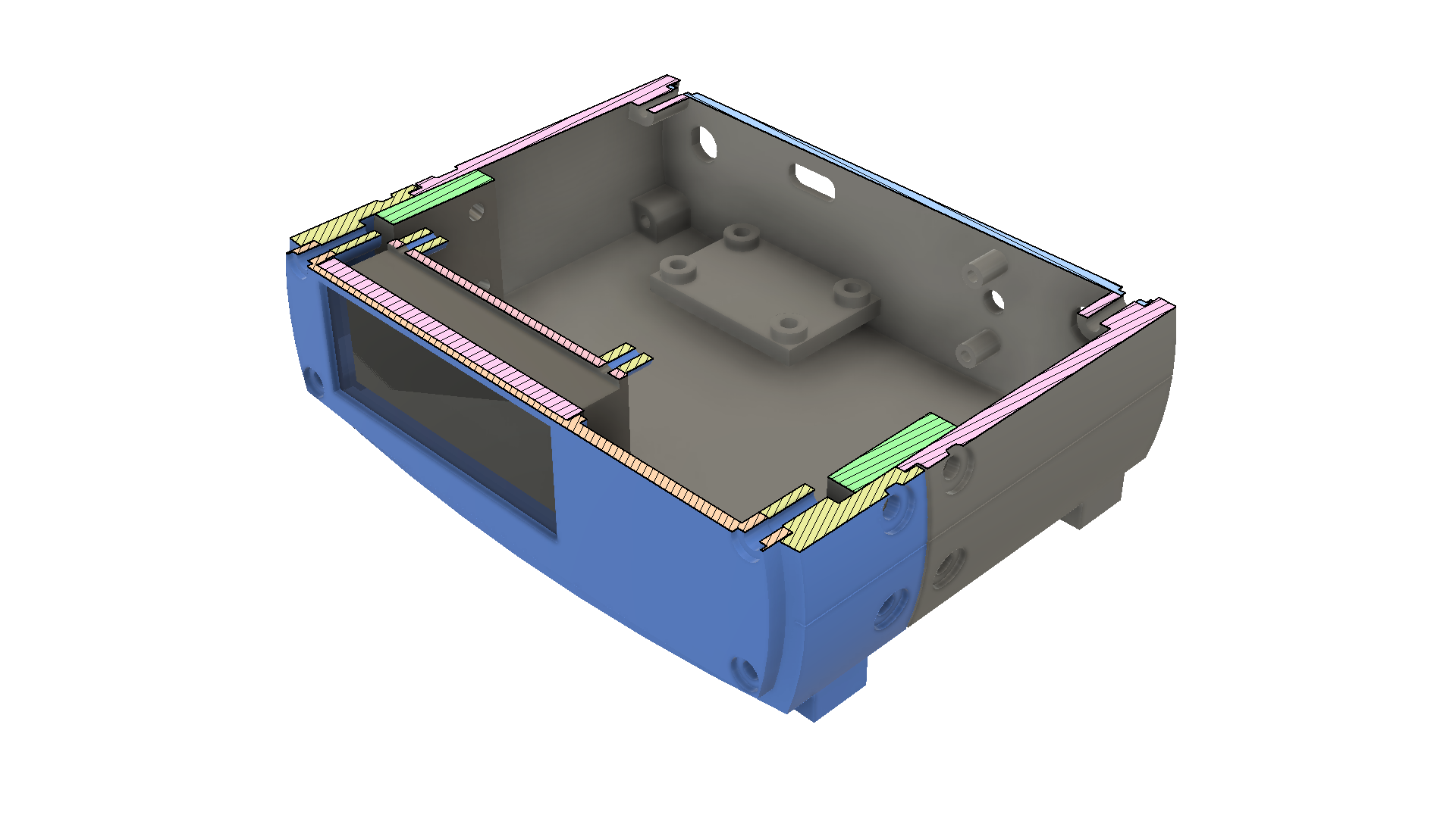
Sectional view of the interior of the router clock 3D model. The acrylic window, display, and mounts for the micro and button boards are visible.
With the circuit boards designed it was time to return to the enclosure and add mounts for the acrylic, display board, button board, carrier board, and Wi-Fi antennas.

The front shell and front panel viewed from the rear of the router clock.
The front panel has an opening for the display and a pocket for the acrylic. The front shell has four mounts for the LCD. All of these features were created by adding their shapes to the initial sketch and then extruding them starting from different offsets from the sketch plane.
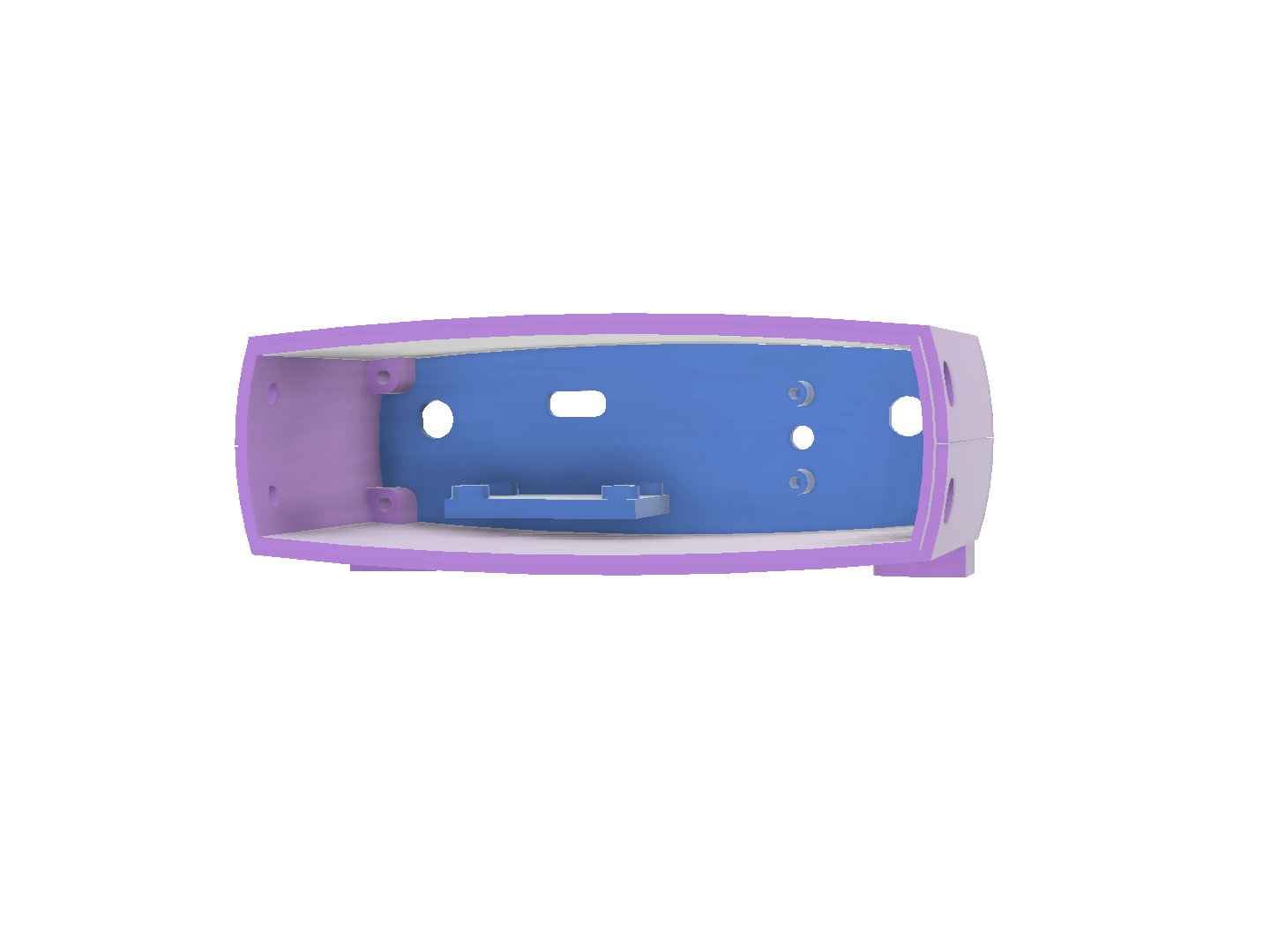
The rear shell and rear panel viewed from the front of the router clock.
The rear panel has holes for the Wi-Fi antennas, USB C port, and button. A shelf with screw holes holds the carrier board. Two more standoffs secure the button board.
Printing the Enclosure
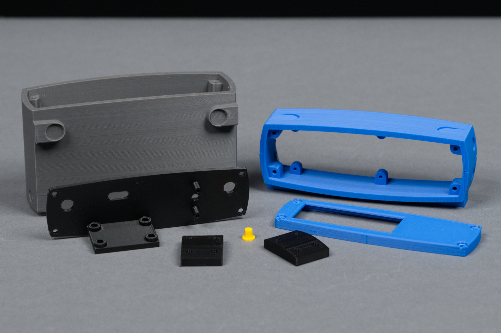
All of the 3D printed plastic components for the router clock.
The photo above shows all the plastic, 3D-printed pieces of the enclosure. I printed these on my Bambu Lab X1 Carbon 3D printer using various colors of their basic PLA filament. Other printer and filament combinations should print fine as well. The design files, in the form of .3mf project files, are available at the end of this post.
Front Shell
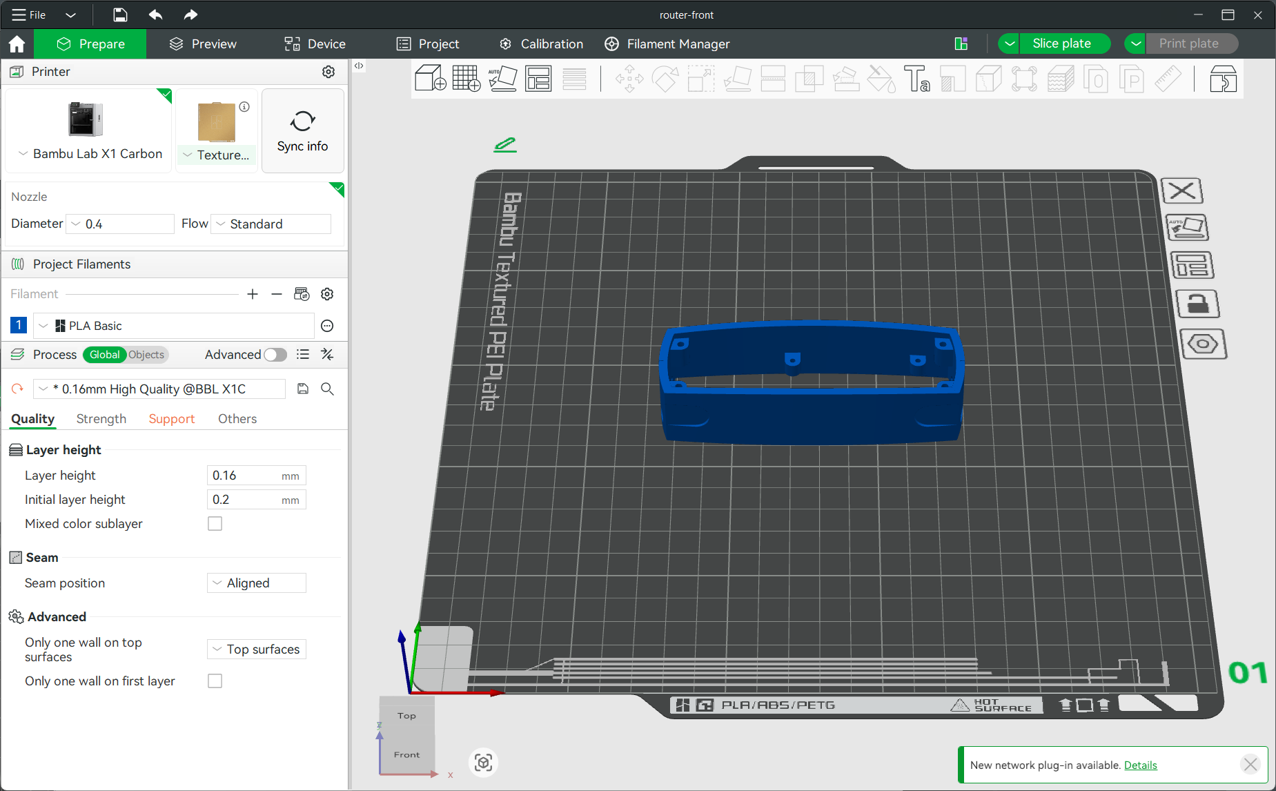
The front shell is printed in Bambu Lab’s cobalt blue basic PLA on a textured build plate.
The front and rear shells are printed separately and upright on the seam where the two shells come together. This is the only planar surface in the shell designs. The front shell is printed from Bambu Lab’s cobalt blue basic PLA using the textured build plate and variable layer thickness is enabled. The .3mf file contains all the settings except possibly the nozzle diameter and build plate type which do not appear to be stored in the file.
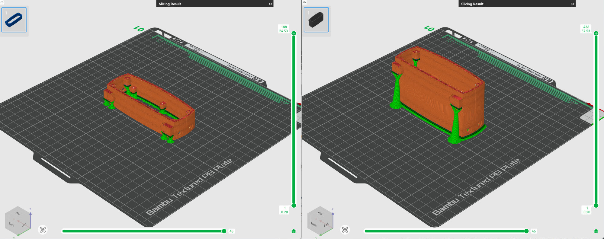
On the left, green supports hold up the inside lip of the front shell. On the right, green supports hold up the outside lip of the rear shell. Once the supports are removed, the shells mesh together to form a single unit.
Since the shells mesh together at the seam, supports must be enabled to fill in material where each half of the shell does not make contact with the print bed. On the front shell, this is along the inside edge of the shell. On the rear shell, this is along the outside edge of the shell. These break off easily and their artifacts are mostly hidden inside the assembled enclosure.
Rear Shell
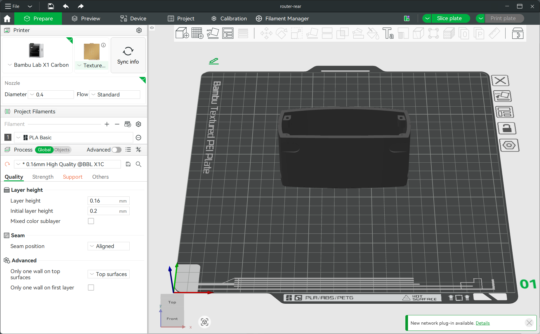
The rear shell is printed in Bambu Lab’s dark gray basic PLA on a textured build plate.
The rear shell is printed from Bambu Lab’s dark gray basic PLA using the textured build plate and variable layer thickness is enabled. Again, support material is required along the outside edge of the shell to support where the front and rear shell mesh together.
Front Panel
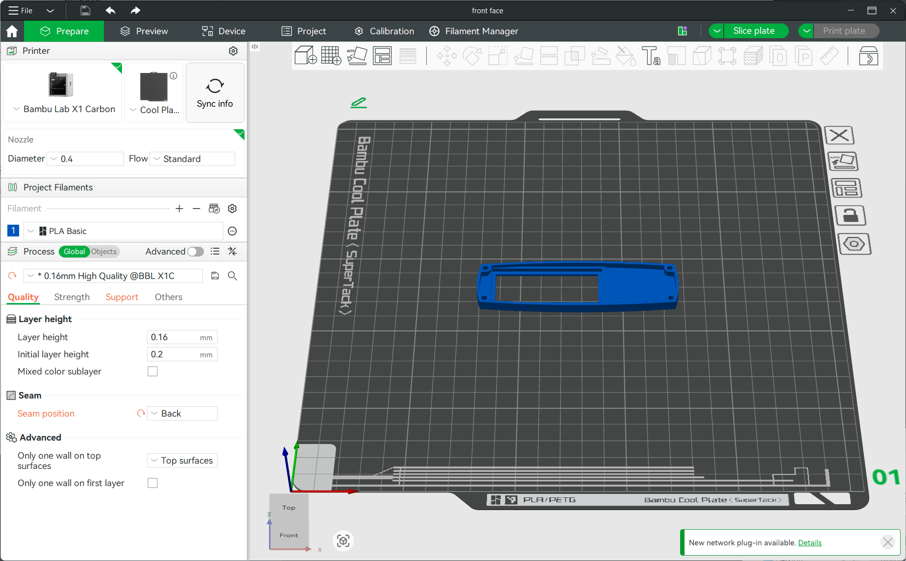
The front panel is printed in Bambu Lab’s cobalt blue basic PLA on a smooth build plate.
The front panel is printed face down and with supports enabled to support the counterbore of the screw holes. It is printed from Bambu Lab’s cobalt blue basic PLA using a smooth build plate. The choice of a smooth build plate was for aesthetic reasons. A textured build plate will work if a smooth build plate is unavailable.
Rear Panel
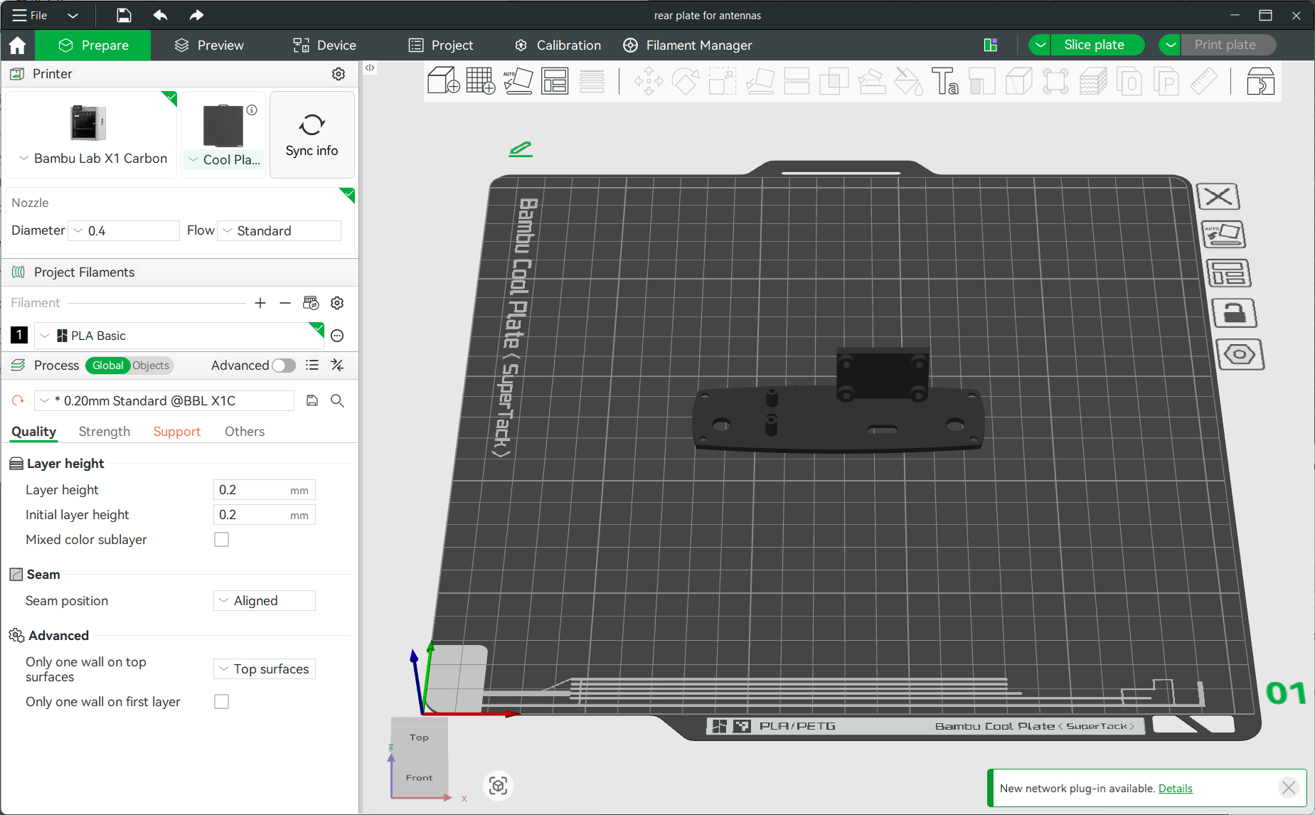
The rear panel is printed in Bambu Lab’s black basic PLA on a smooth build plate.
The rear panel is printed face down and with supports enabled to support the counterbore of the screw holes and the recess around the USB C port. It is printed from Bambu Lab’s black basic PLA using a smooth build plate. The choice of a smooth build plate was for aesthetic reasons. A textured build plate will work if a smooth build plate is unavailable.
Joiners
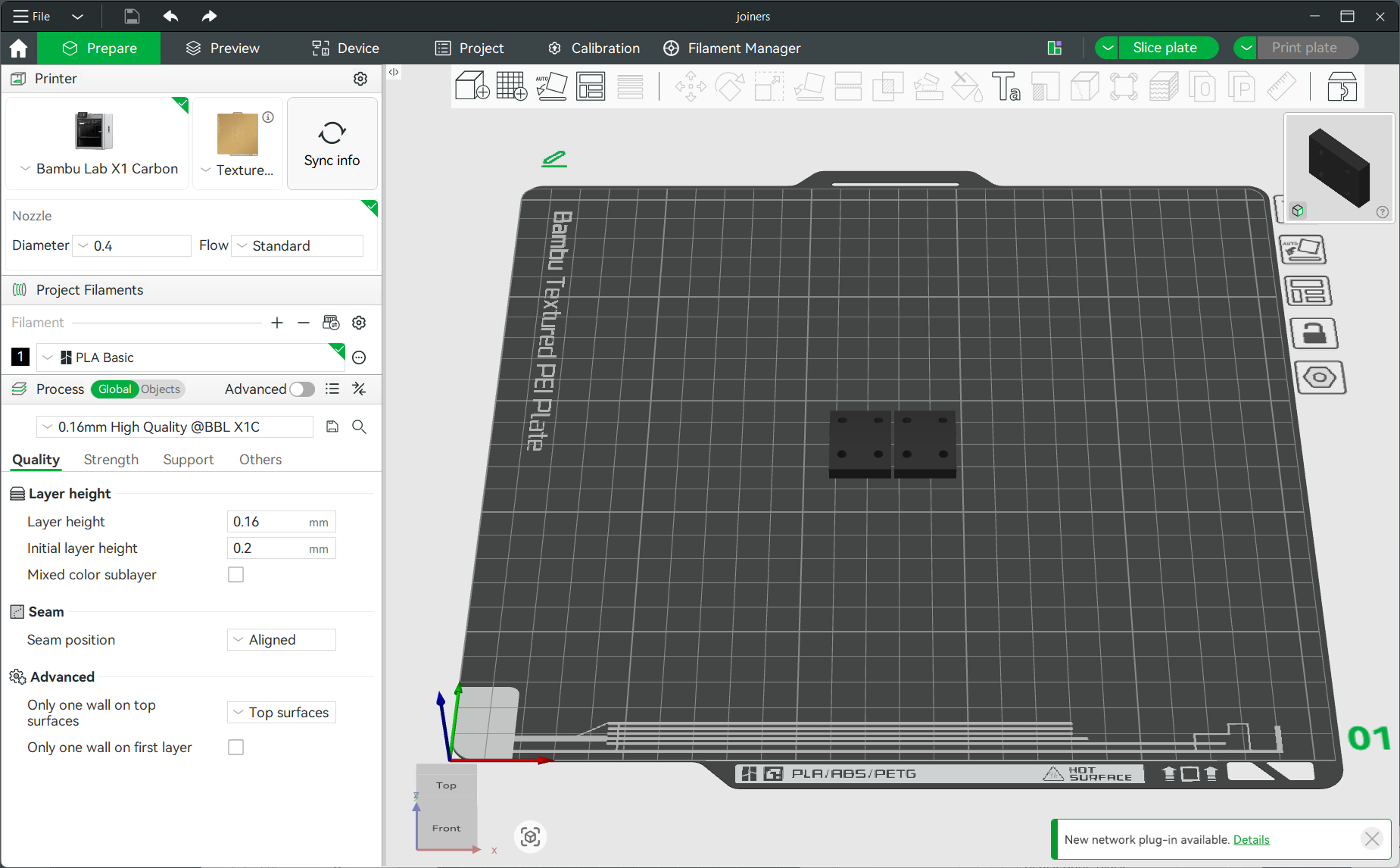
The joiners are printed in Bambu Lab’s black basic PLA on a textured build plate.
The joiners hold the front and rear shells together. These are printed using Bambu Lab’s black basic PLA and a textured build plate. They’re completely hidden in the assembled design so feel free to use that color you hate or any leftover scraps.
Switch Plungers

The switch plungers are printed in Bambu Lab’s sunflower yellow basic PLA on a textured build plate.
The switch plunger extends through the rear panel to allow the tactile switch to be pressed. I printed these in Bambu Lab’s sunflower yellow basic PLA on a textured build plate.
Software
The software has two main modes. The first mode, access point or AP mode, is entered when the button on the rear of the clock is held down during startup. The second mode, normal mode, is entered otherwise. In AP mode, the Wi-Fi network, time server, and time zone can be configured. In normal mode, the clock attempts to connect to the configured Wi-Fi network and retrieve the time from the configured NTP server.
AP Mode
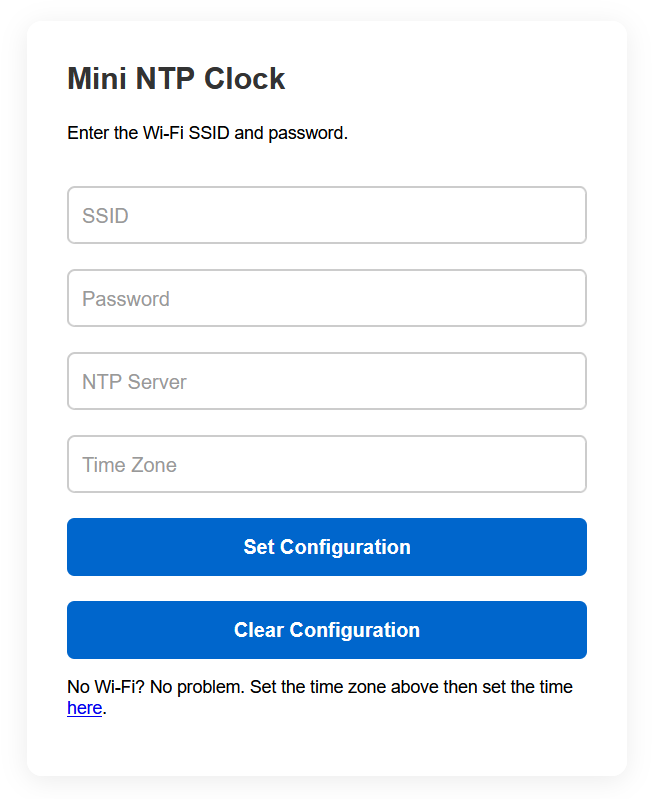
The configuration screen in AP mode.
AP mode is entered by holding down the button on the rear of the clock. When AP mode is activated, the display will show “AP” and a Wi-Fi access point named “ESP32 Mini NTP Clock” is created. Most phones and laptops will recognize this as a network that requires a login to access the internet and automatically redirect to the webpage shown above. If not, the page can be accessed at 192.168.4.1.
On this page, enter the Wi-Fi SSID and password, a time server such as pool.ntp.org, and the timezone string. The timezone string conforms to the POSIX time zone specification. A good reference including many pre-formatted timezone strings can be found on this page. As an example, the timezone string for Denver is MST7MDT,M3.2.0,M11.1.0. Be careful there are no extra spaces after each entry.
Once the data is entered, click “Set Configuration” to store the configuration in the clock. The clock can now be restarted by cycling power (like Kyle in the South Park episode) to join the network and retrieve the time.
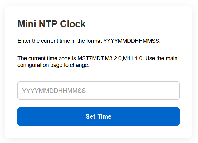
Manually setting the date and time without a Wi-Fi network or time server.
If the clock is located somewhere without Wi-Fi or where the Wi-Fi is inaccessible like on a corporate network, don’t fret, the time can be set manually. Place the clock in AP mode and click the link below the “Clear Configuration” button to be directed to the screen above. Enter a time string like “20261201135923” and click “Set Time.” The clock will then immediately set and display the time without attempting to connect to a network or server. This example sets the date and time to 1:59:23 PM on December 1, 2026.
Normal Mode
In normal mode, the clock will blink “12:00″ as a homage to the good old VCR clock until the Wi-Fi is connected and the NTP time is retrieved. Once both are ready, the time will display in 24 hour format. If the Wi-Fi connection or time is lost, the clock should return to blinking “12:00″ until it can reconnect and retrieve the time again.
Compiling
The software was written for the Arduino development environment. A Makefile is included for compiling and downloading with the Arduino CLI, but the Arduino IDE should work too. The arduino-timer and HT16K33 libraries are required.
Programming Notes
Note that the initial programming of the XIAO board with the Arduino environment requires holding down the ‘B’ button while pressing and releasing the ‘R’ button. This is easier to do before the project is assembled so program the XIAO board with the Arduino environment at least once before assembling the project.
Bill of Materials
The bill of materials is listed below. It is divided into separate sections for each part of the assembly.
Button Board
| Qty | Description | Manufacturer | Part Number |
| 1 | button board PCB | DKRed | custom |
| 1 | JST SH 4-pin right-angle header | JST | SM04B-SRSS-TB |
| 1 | tactile switch | Omron | BSF-1006 |
| 1 | 50 mm QWIIC cable | Sparkfun | PRT-17260 |
Display Board
| Qty | Description | Manufacturer | Part Number |
| 1 | 0.56″ green clock display w/ IIC backpack, assembled | Adafruit | 5603 |
| 1 | 100 mm QWIIC cable | Sparkfun | PRT-17259 |
Carrier Board
| Qty | Description | Manufacturer | Part Number |
| 1 | carrier board PCB | DKRed | custom |
| 1 | Seeed XIAO ESP32-S3 | Seeed | 113991114 |
| 2 | JST SH 4-pin right-angle header | JST | SM04B-SRSS-TB |
| 1 | PCA9306 SOIC-8 | TI | PCA9306DCTR |
| 1 | 0603 200 kΩ | generic | — |
| 1 | 0603 100 pF | generic | — |
| 2 | short headers, 7 pin | Adafruit | 3009 |
| 2 | short header sockets, 7 pos | Samtec | CES-107-01-T-S |
Hardware and Misc
| Qty | Description | Manufacturer | Part Number |
| 6 | M2 x 6 mm button head screw | generic | Buy from Amazon* |
| 4 | M3 x 4 mm button head screw | generic | Buy from Amazon* |
| 8 | M3 x 6 mm button head screw, black finish | generic | Buy from Amazon* |
| 8 | M2.5 x 6 mm socket head screw, black finish | generic | Buy from Amazon* |
| 1 | 54 x 23 x 3 mm transparent dark gray acrylic sheet | SendCutSend | custom |
| 2 | Short, right-angle, RP-SMA Wi-Fi antennas | generic | Buy from Amazon* |
| 2 | RP-SMA to u.FL panel mount cable assemblies | generic | Buy from Amazon* |
| 4 | Rubber foot, round, 0.315″ diameter | 3M | SJ5076 |
*affiliate link: I will earn a small commission from Amazon if these parts are purchased using the links.
3D Printed Parts
The section below lists the 3D printed parts, their build plates, and their filaments. The design files themselves are located at the end of this post.
| Qty | Description | Build Plate | Filament |
| 1 | front panel | smooth | cobalt blue |
| 1 | front shell | textured | cobalt blue |
| 1 | rear panel | smooth | black |
| 1 | rear shell | textured | dark gray |
| 1 | button plunger | textured | sunflower yellow |
| 2 | joiners | textured | black |
Assembly
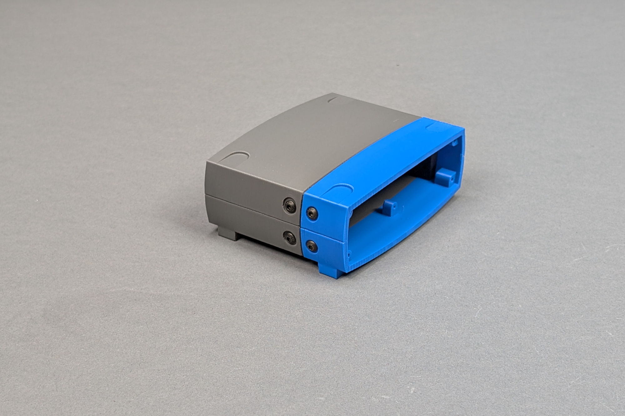
1) Attach the joiners to the rear shell using four of the M3 x 6 mm screws.

2) Attach the front shell to the joiners and rear shell using the last four M3 x 6 mm screws.
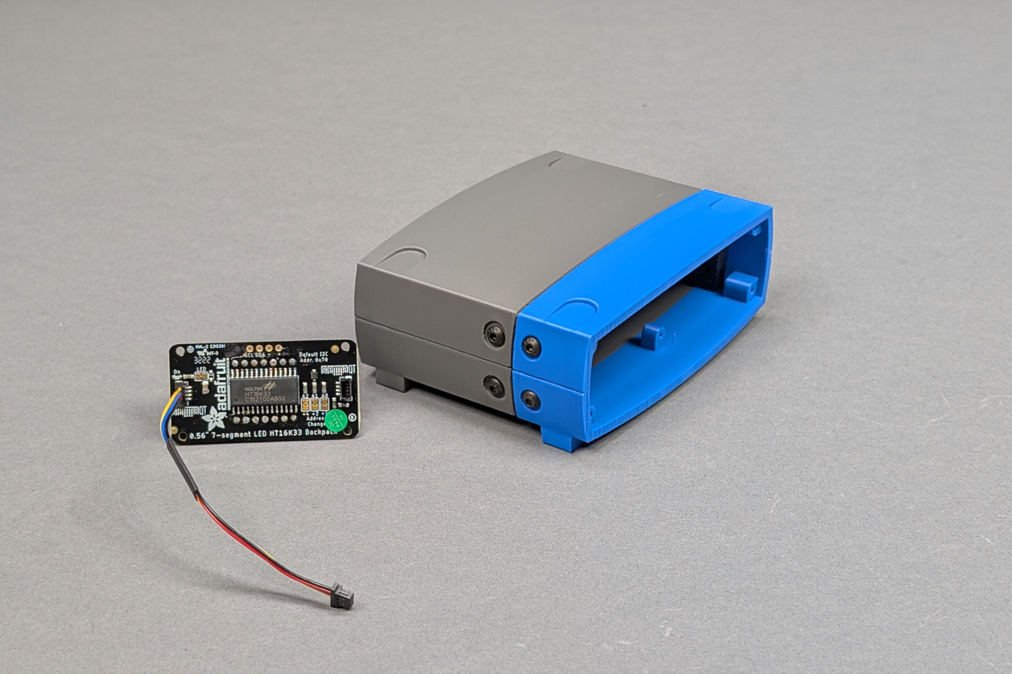
3) Attach the 100 mm QWIIC cable to the display’s left JST connector as viewed from the rear of the display.
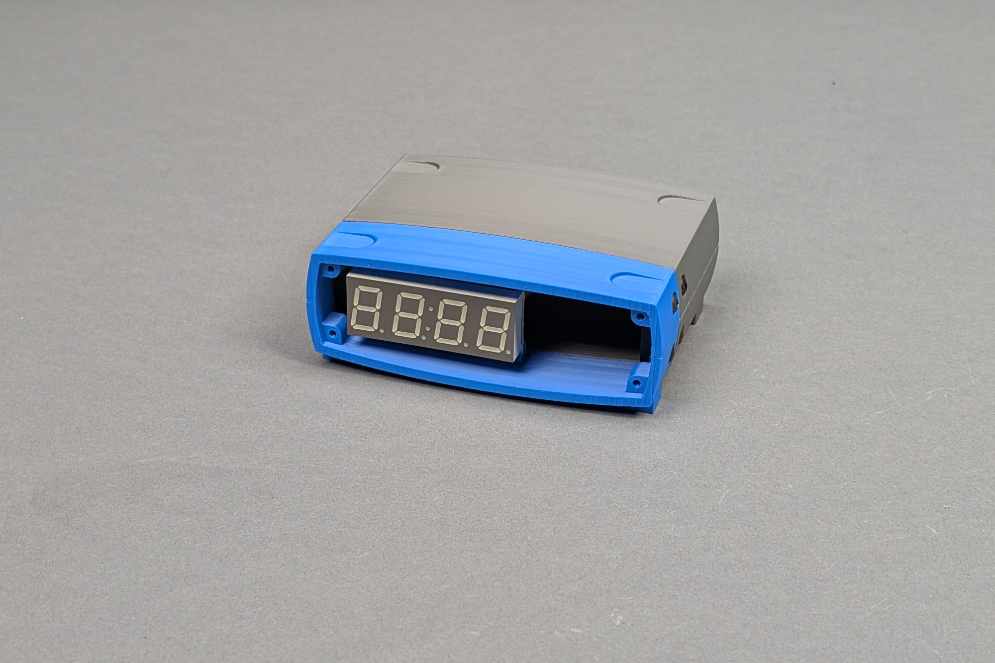
4) Mount the display to the front shell using four of the M2 x 6 mm screws and route the QWIIC cable out the rear of the enclosure.
5) Remove the protective paper and insert the acrylic window into the front panel pocket.
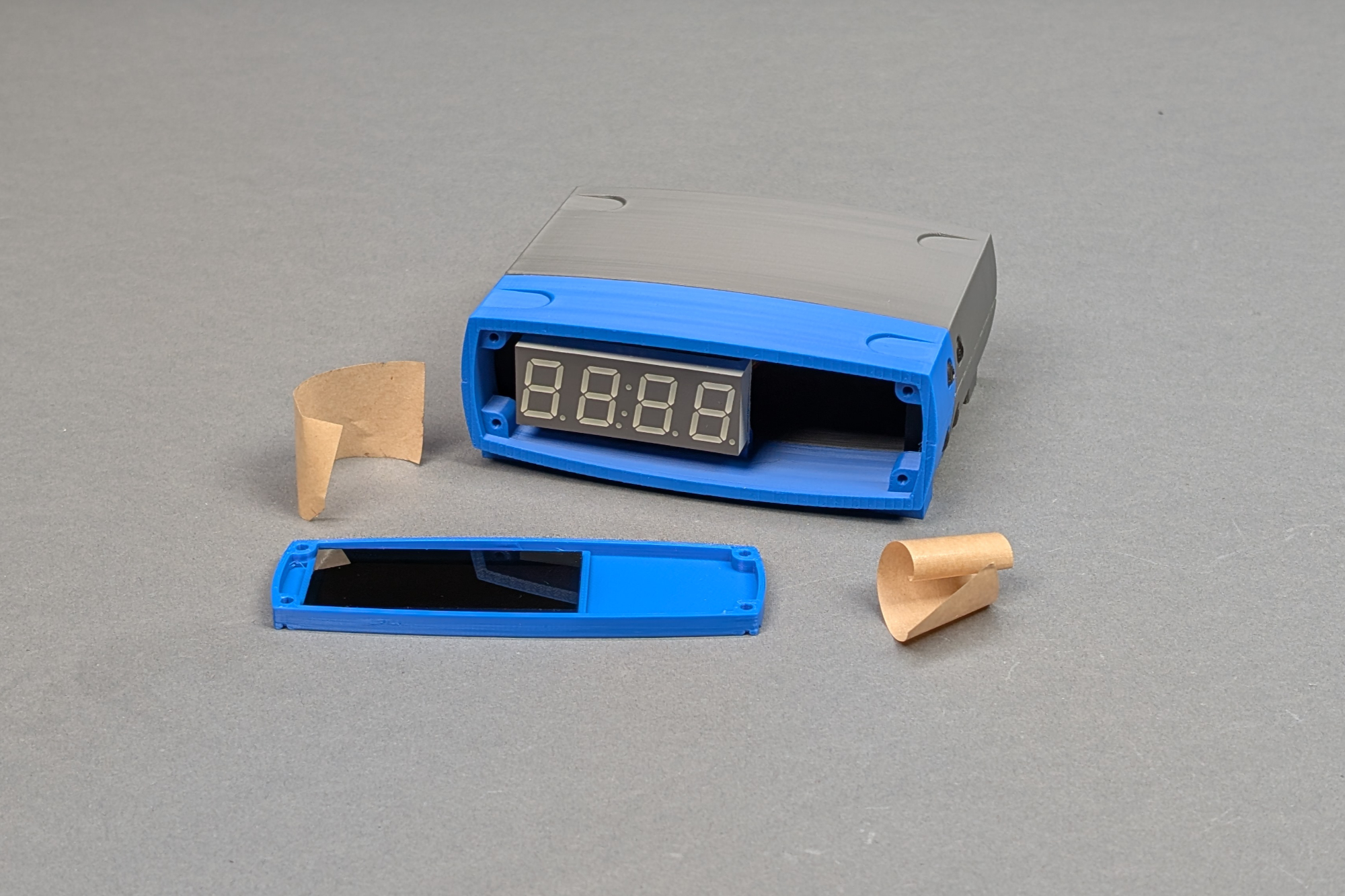
6) Mount the front panel to the front of the enclosure using four of the M2.5 x 6 mm socket head cap screws.
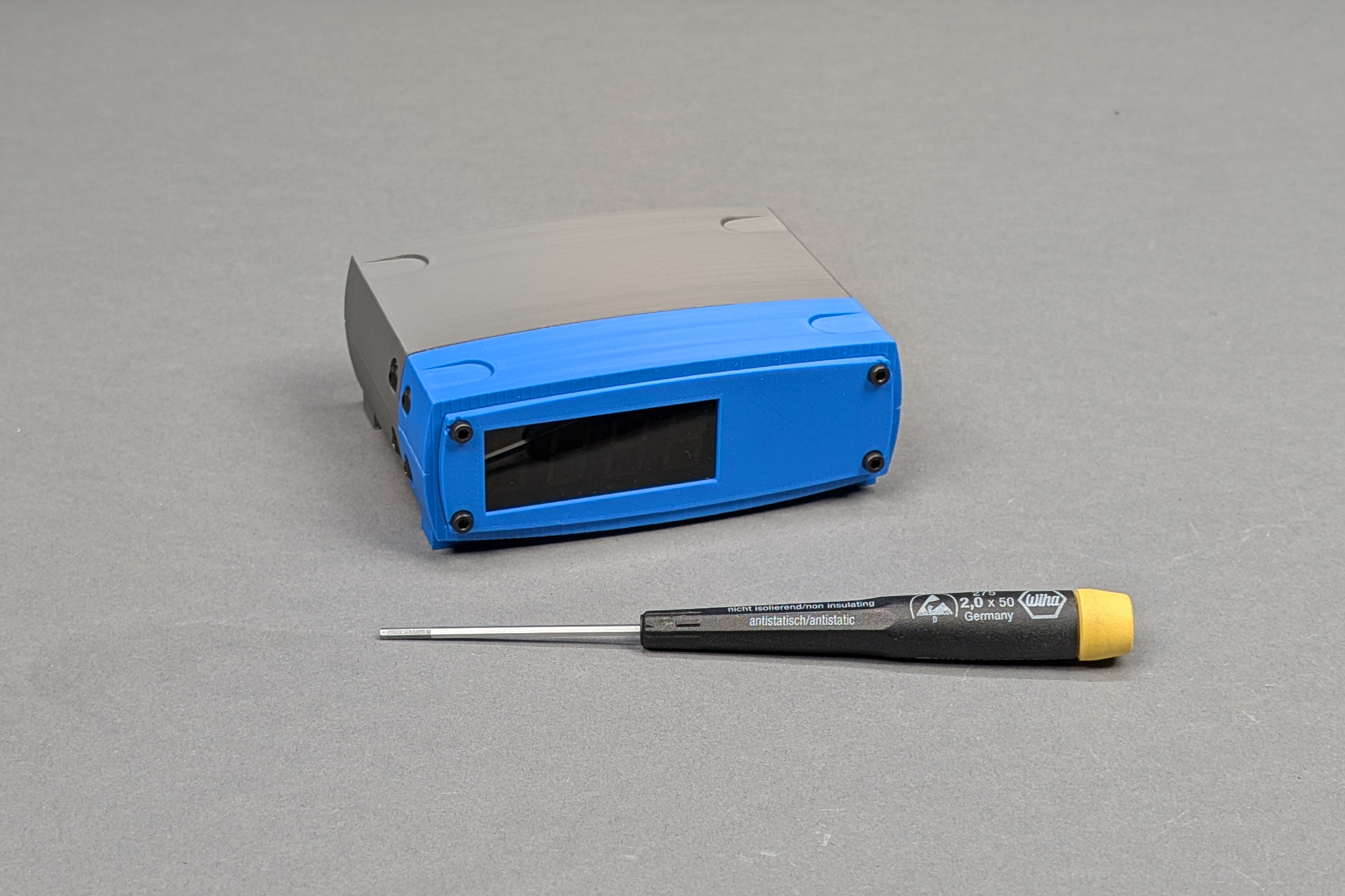
7) Push the plunger through the rear panel.
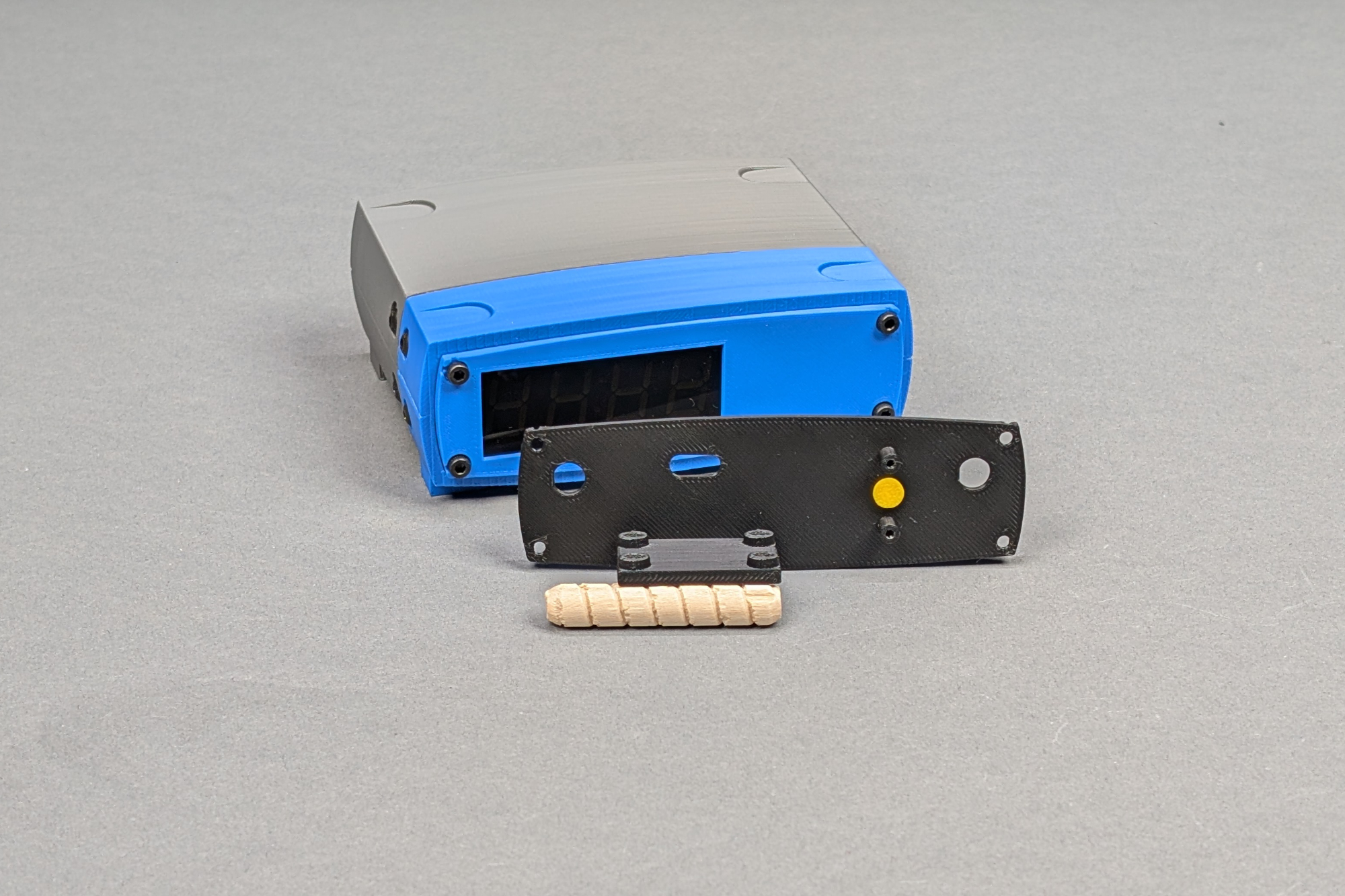
8) Mount the assembled button board to the rear panel using the two remaining M2 x 6mm screws.
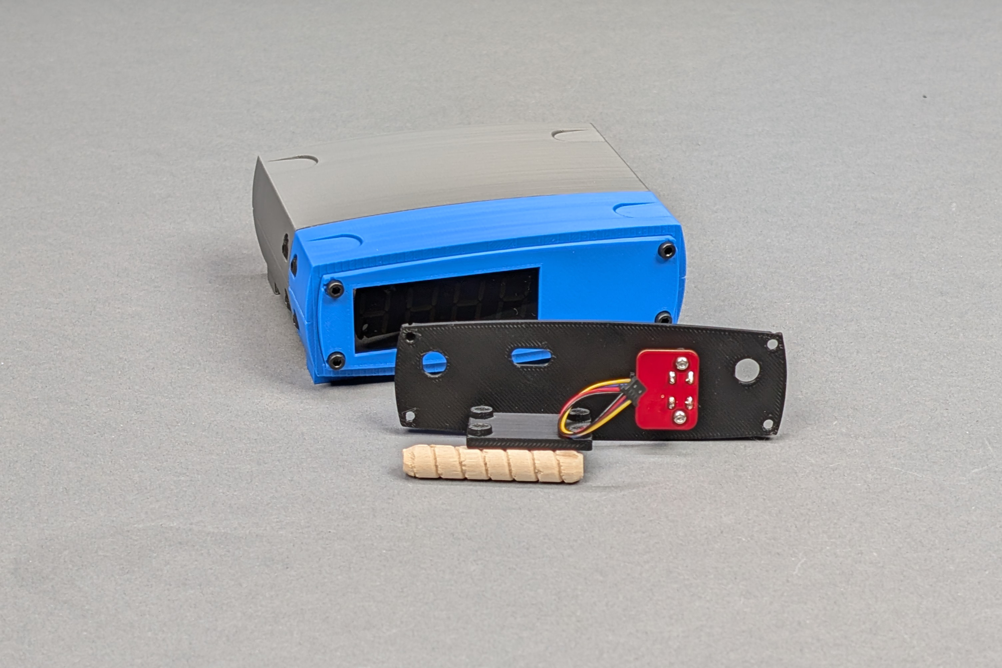
9) Connect the 50 mm QWICC cable from the button board to the side QWIIC connector on the carrier board and mount the carrier board to the rear panel using the four M3 x 4 mm screws.

10) Mount the two SMA antenna cables on the rear panel.

11) Connect one SMA antenna cable to the XIAO board on the carrier board. Cut the other SMA antenna cable at the connector to prevent shorts.
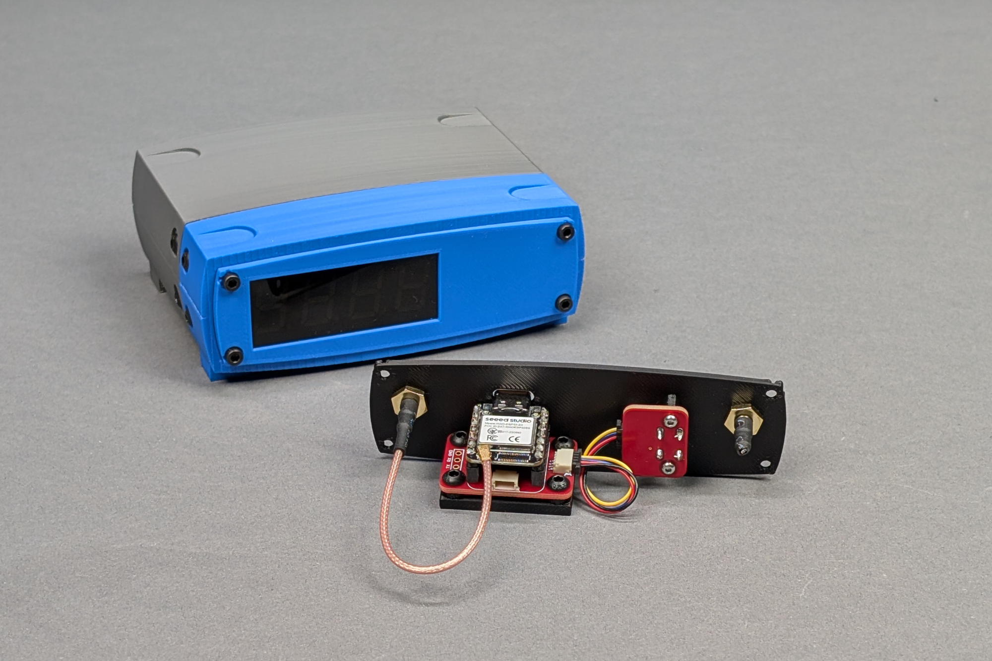
12) Thread the antennas on to the SMA connectors and connect the display’s QWICC cable to the rear QWIIC connector on the carrier board.

13) Install and test the software.
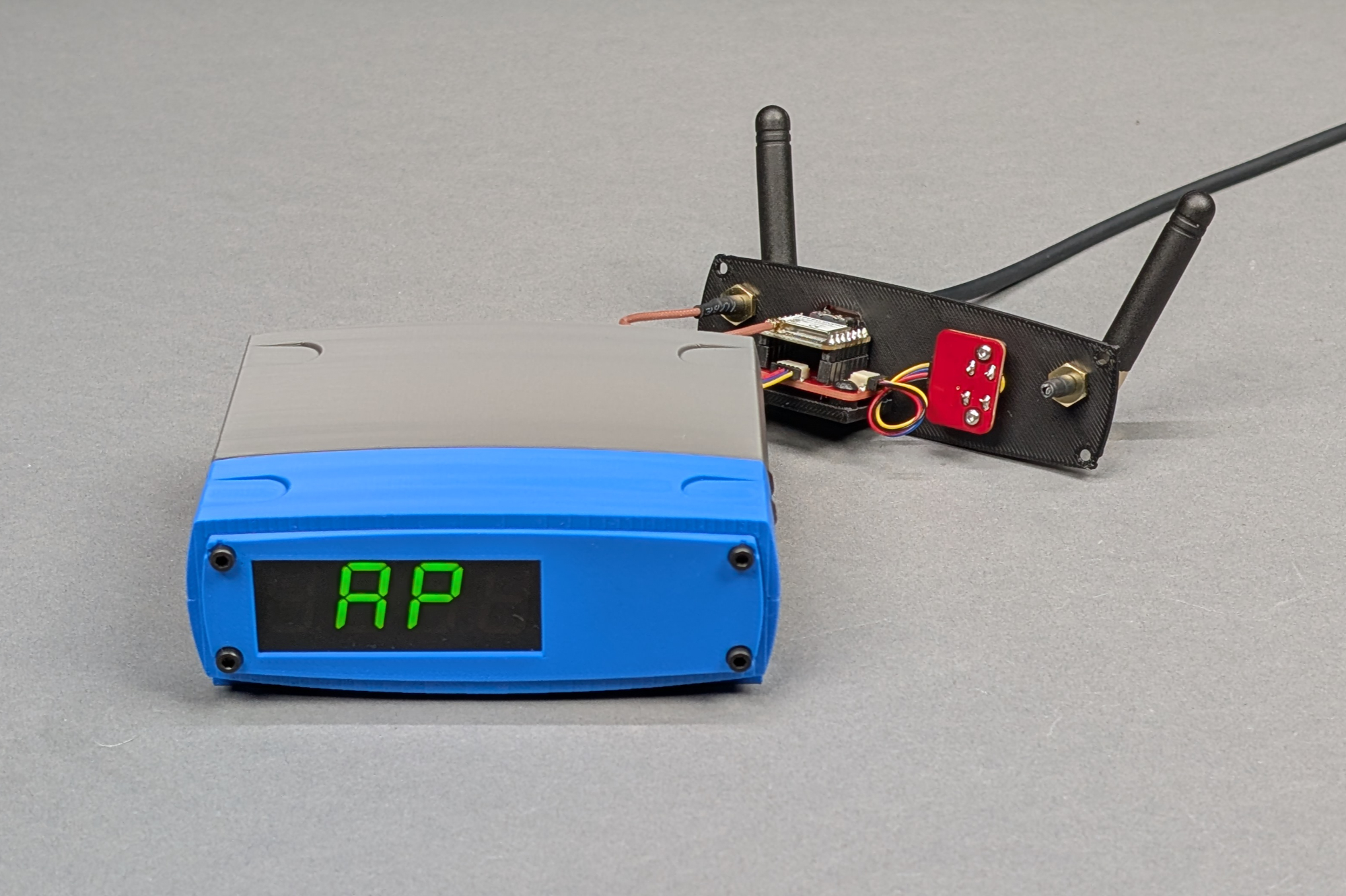
14) Mount the rear panel to the rear shell using the four remaining M2.5 x 6 mm socket head cap screws.
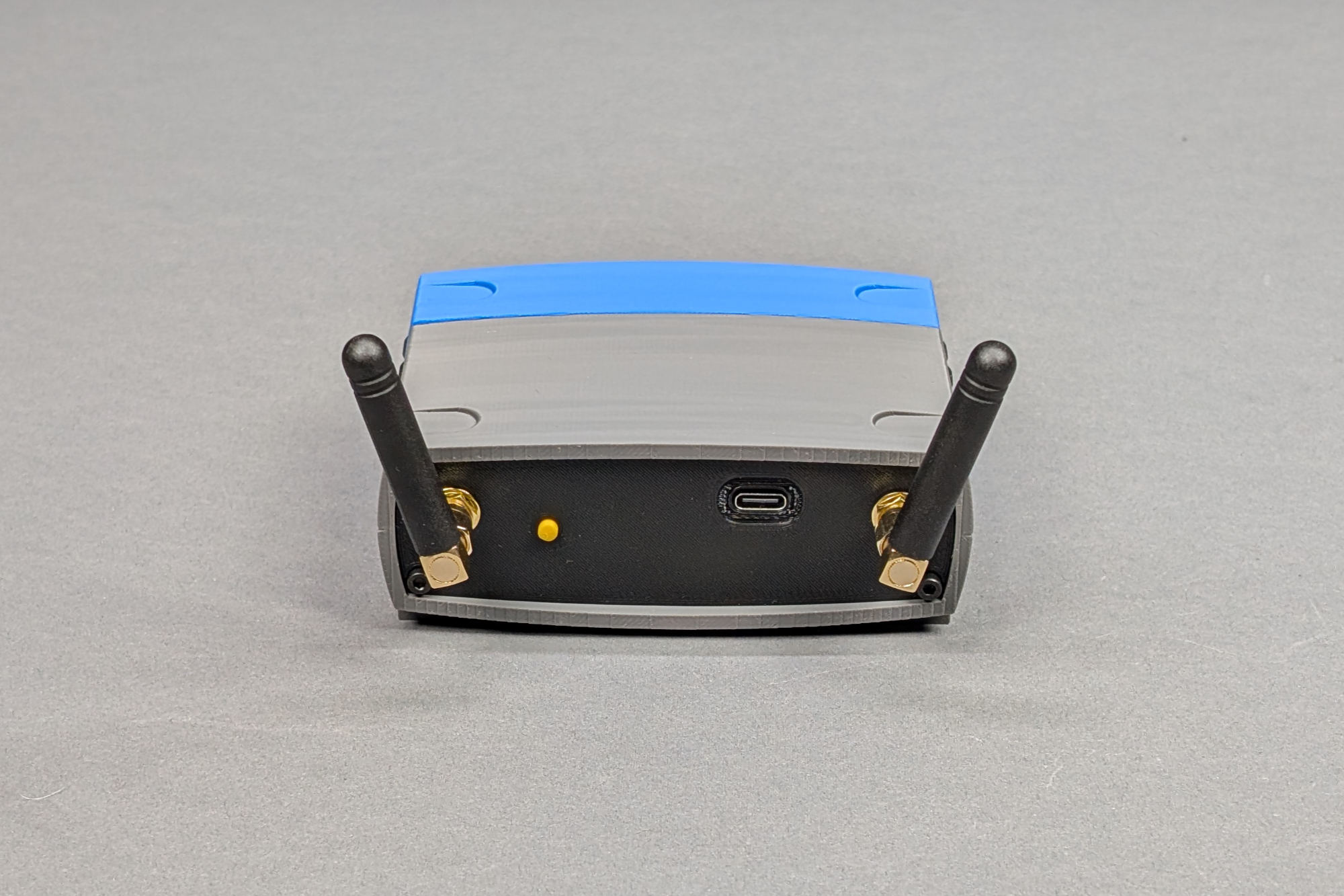
15) Stick the four rubber feet to the bottom of the enclosure.
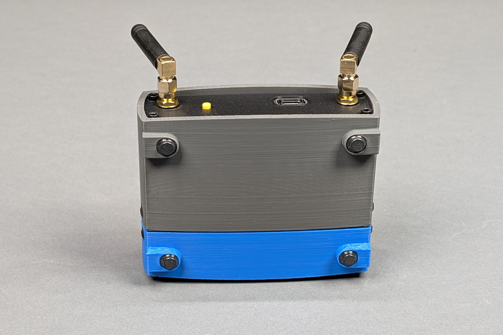
16) Move the antennas to their final position, power up, and configure the clock.

Optional Decals
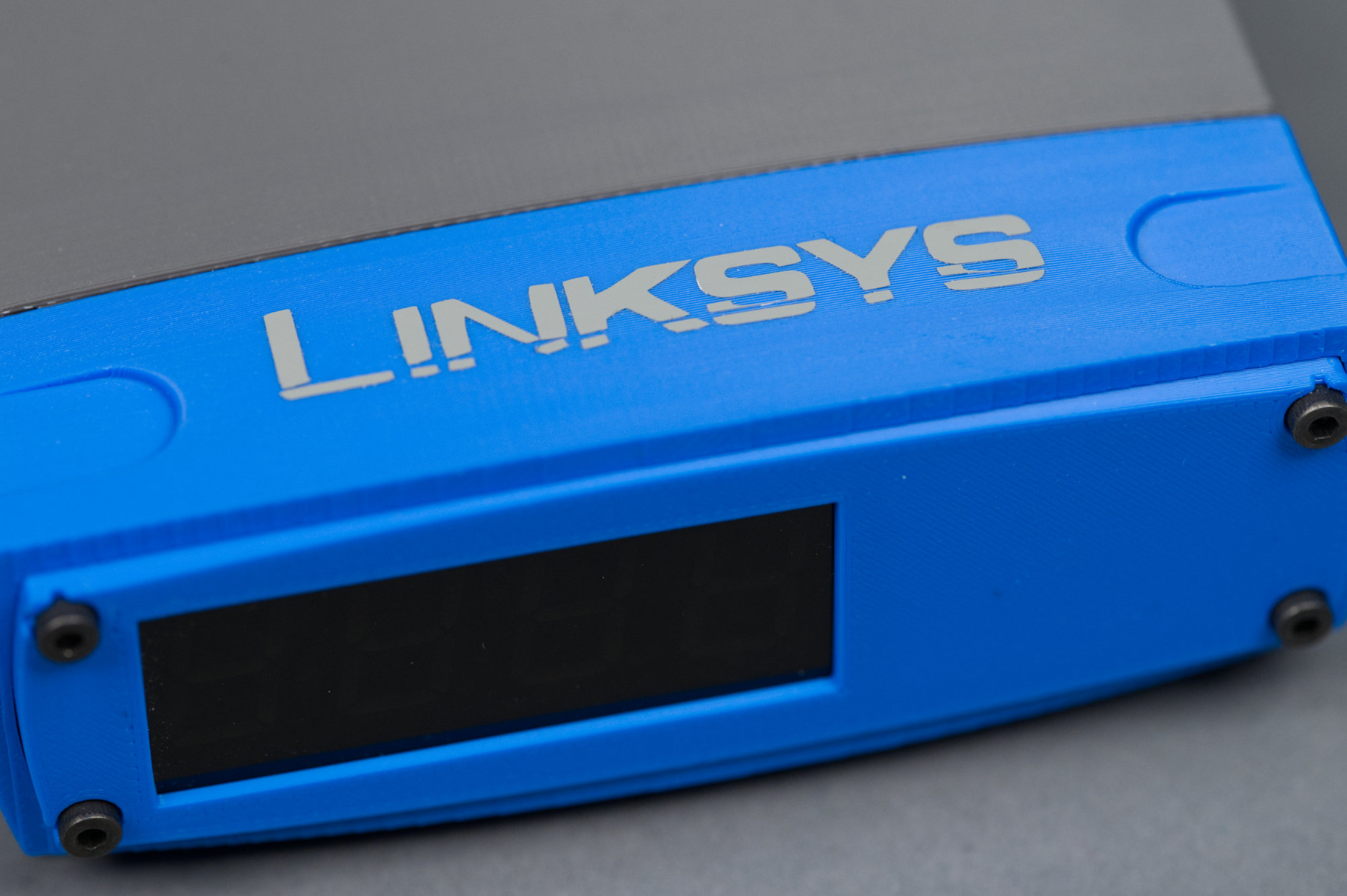
Not the best vinyl application ever but it’s fine at a distance.
I used a Silhouette vinyl cutter and this Linksys logo file from Wikimedia Commons to cut a Linksys logo sticker for the top of my router clock. Without the circled-R registered trademark symbol, the logo is 55 mm wide. I used Oracal 651 glossy permanent middle grey vinyl for the logo sticker. The logo at this size is very detailed. The bulk of the logo transferred from the transfer tape well but a few parts had to be removed and individually replaced with parts from a second cut sticker.

Assembled Photos
Here’s a few more pictures of the assembled router clock.
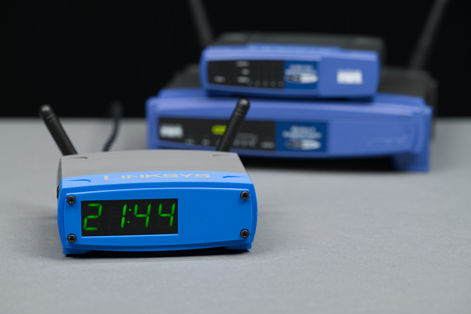
The completed clock in front of a 5-port switch and a wireless router.
The router clock is complete!
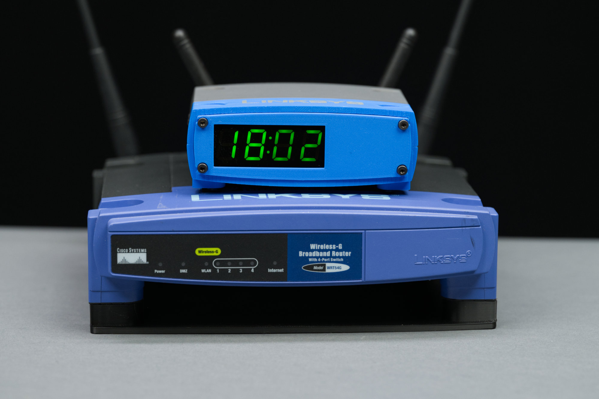
The router clock on top of my WRT-54G wireless router.
Close enough!
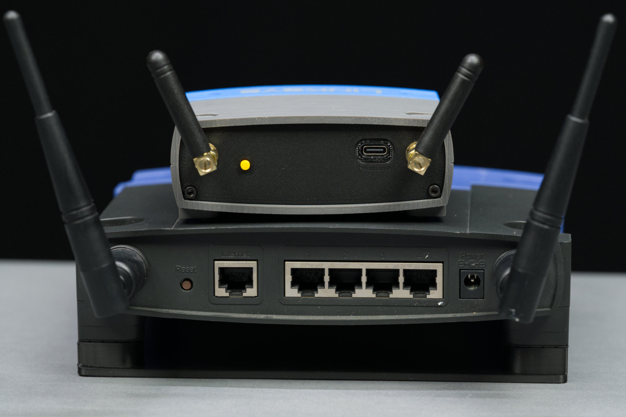
Rear view of the router clock and the WRT-54G wireless router.
Completely different from the back!
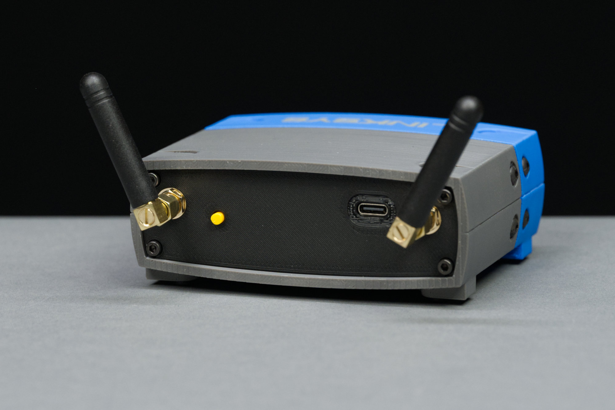
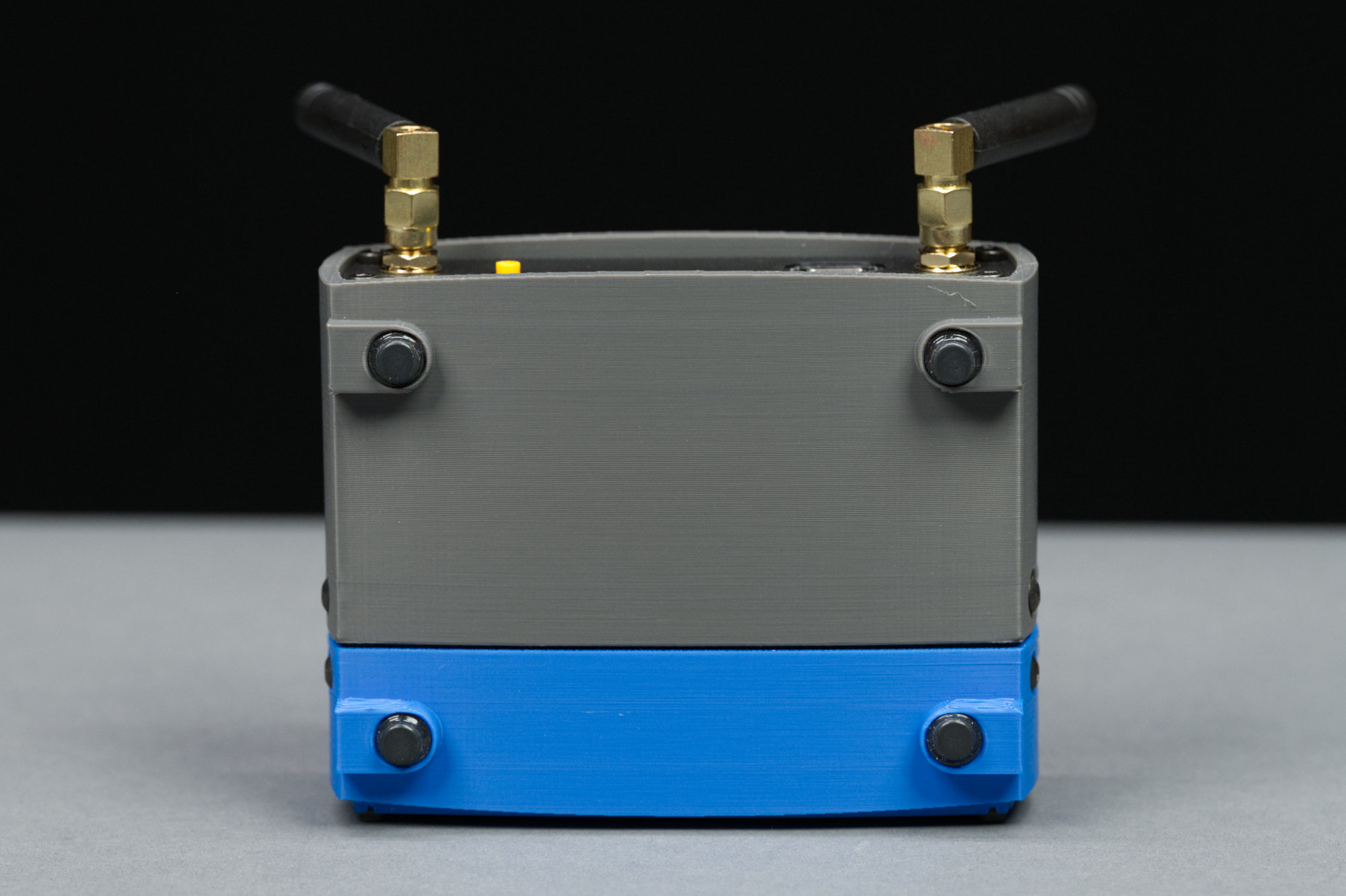
Rear view showing the antenna connectors, AP mode button, and USB type C power / programming connector.
Another view of the rear of the router clock.
The bottom of the router clock.
A view of the bottom showing the rubber feet and the indents in the router’s feet for the rubber feet. From this view, the curvature of the front and back shells is clearly visible.
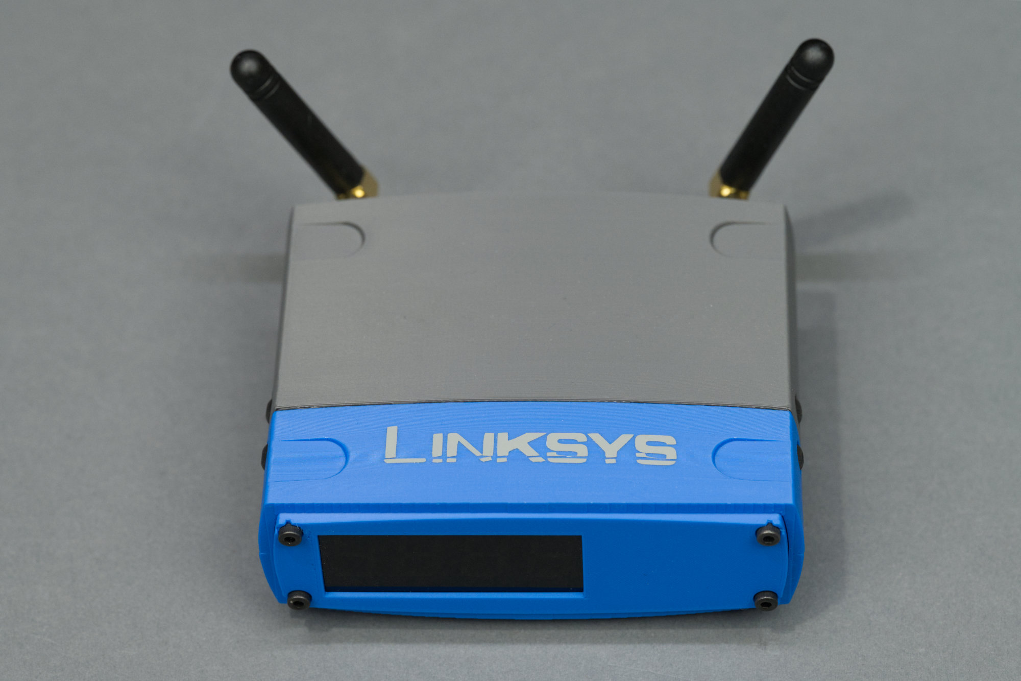
Overhead view of the router clock
An overhead view of the router clock.
Bonus Content: Making a Stackable Enclosure
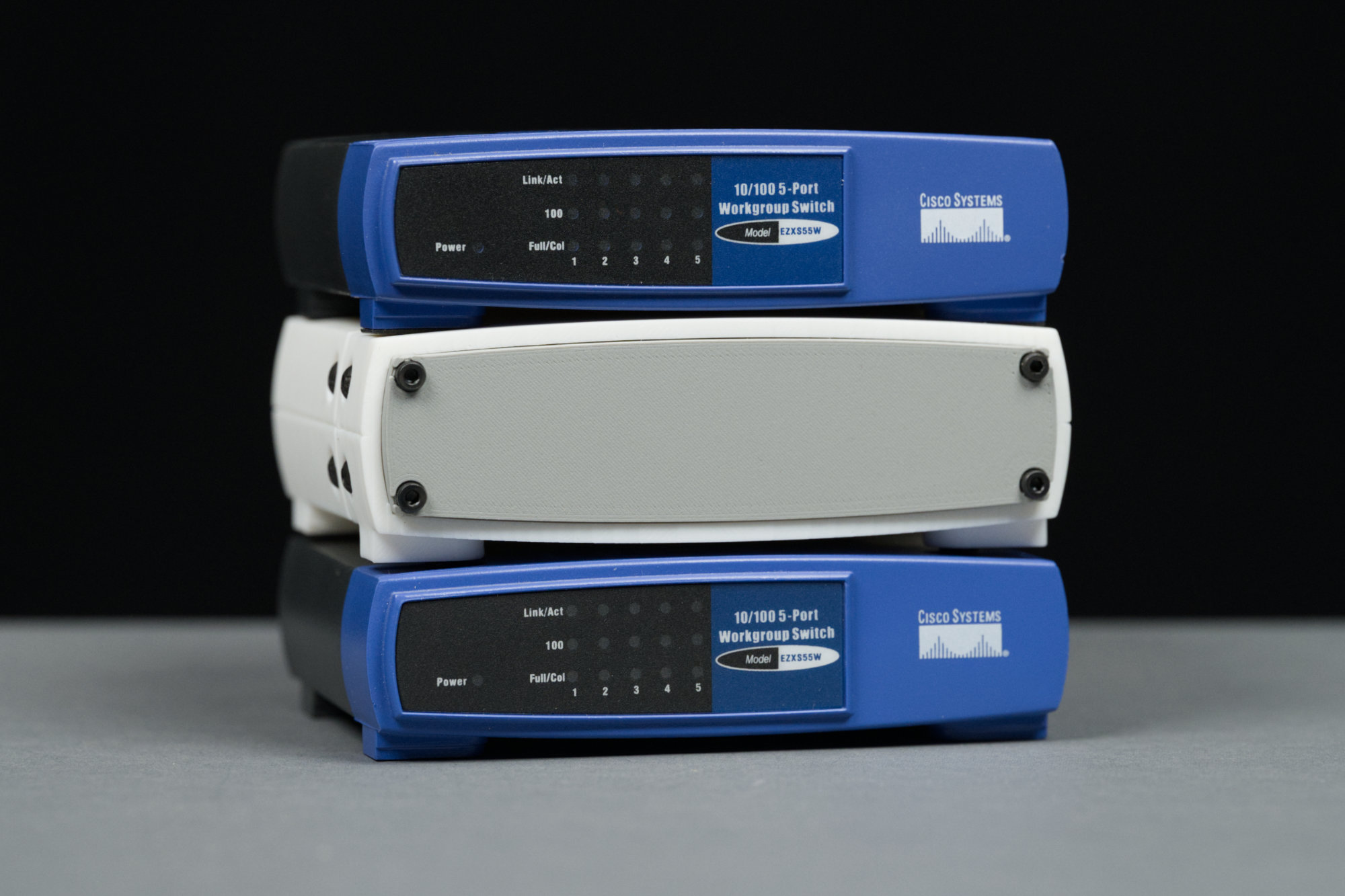
A stackable version of the enclosure sandwiched between two 5-port workgroup switches.
I did make a stackable version of the enclosure to prove that it could be done. After measuring the feet of a 5-port workgroup switch with a set of calipers and making a few test prints, I came up with the design shown above.
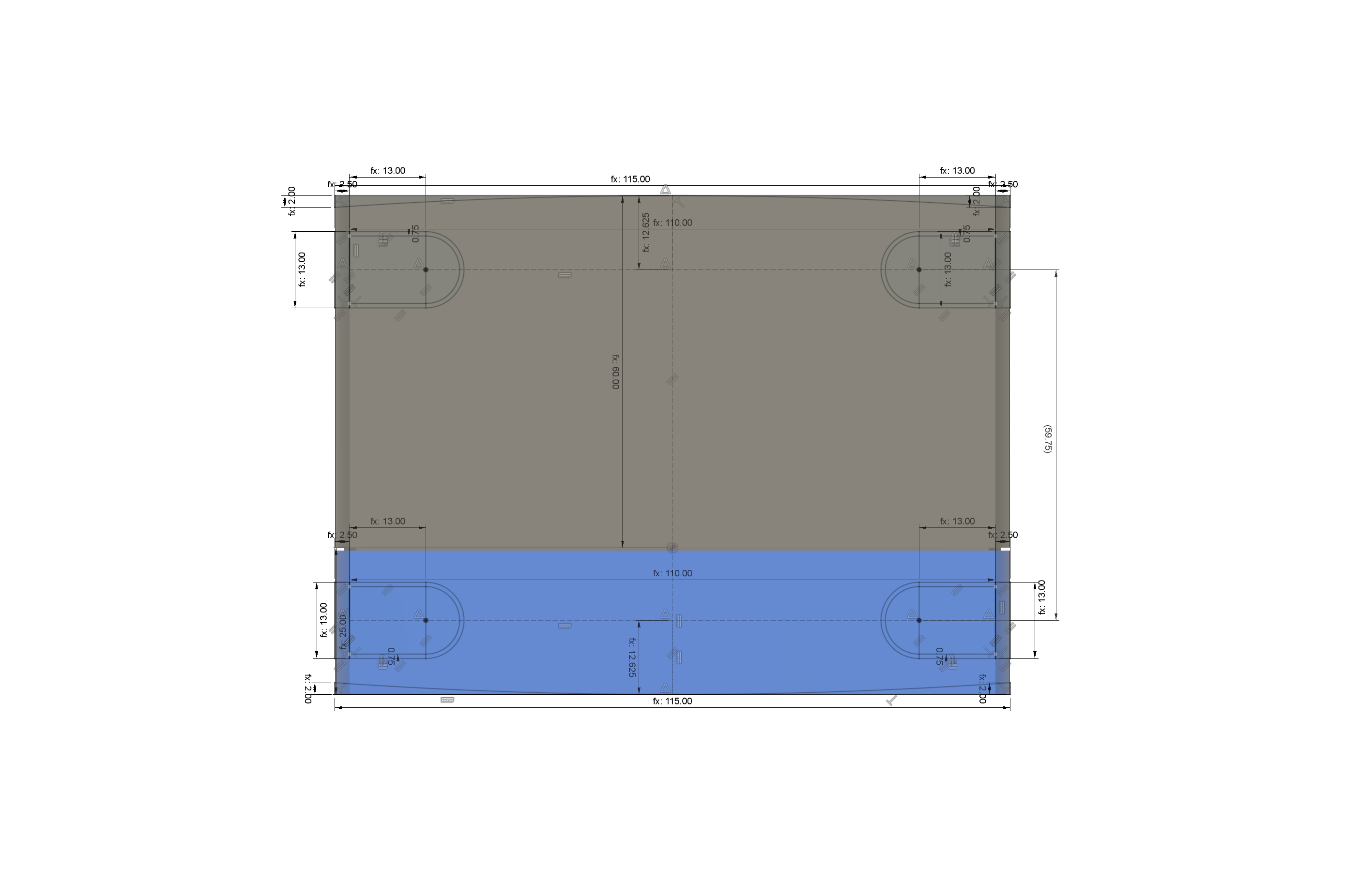
The dimensions of the stackable version of the enclosure.
The rear shell was extended from 55 mm deep to 60 mm deep and the width was expanded from 100 mm to 110 mm. The foot offset had to be reduced to 4.125 mm and the foot diameter increased to 13 mm. With those parameter changes, a 5-port workgroup switch could be stacked on top of the enclosure. To make the enclosure able to stack on top of a 5-port workgroup switch, I had to inset the feet 0.75 mm. The inset was the only non-parameterized change required to resize and make the enclosure stackable.
Design Files
The design files are available for your personal, non-commercial use subject to the terms of Creative Commons CC BY-BC-SA 4.0 license.
- 3D Printed Parts:
- Laser Cut Parts:
- Button Circuit Board:
- Carrier Circuit Board:
- Software: