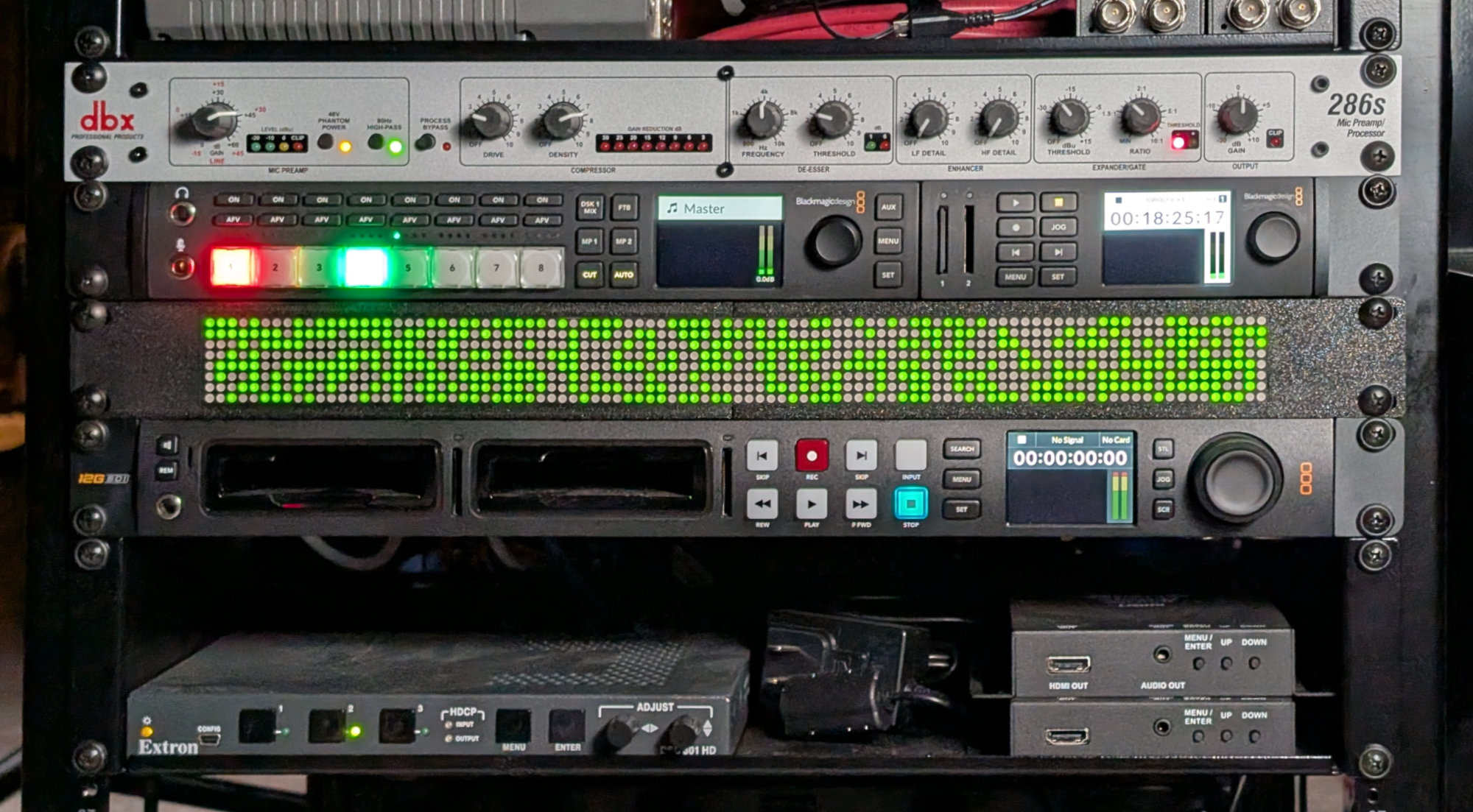
The WOPR LED display makes a nice filler panel in an otherwise very dusty rack of equipment.
This was supposed to be a simple project. I already had a set of 12 8×8 LED matrix modules, software, and a micro. All I had to do was print out a .3mf file, slide the modules into the prints, tighten some screws, and flash some software. The project ended up being anything but simple. Read on to find out what went wrong and how I got things back on track.
The Initial Few Tries
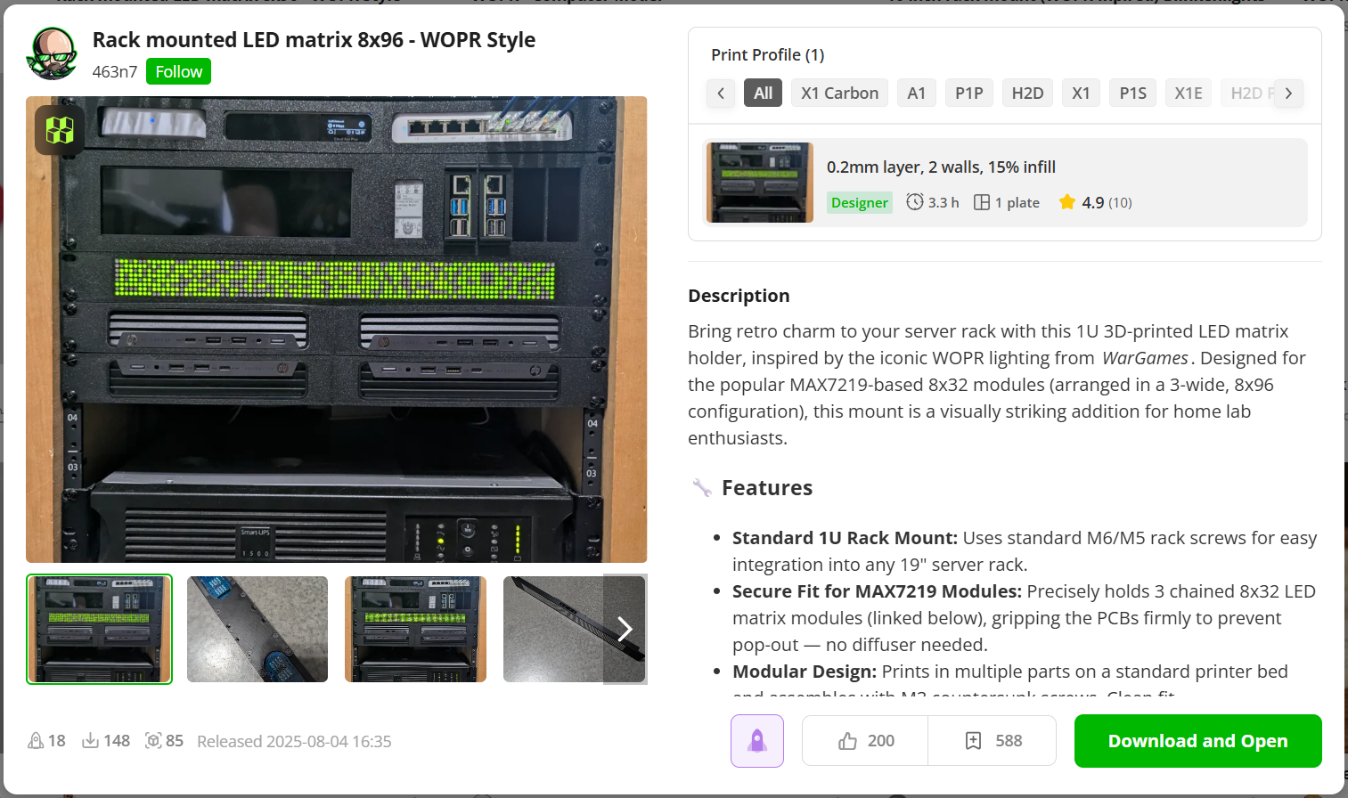
Cover page for the WOPR project on Bambu Lab’s MakerWorld.
I found this WOPR LED project on MakerWorld and thought to myself “I have a 3D printer! I have a bunch of MAX7219 modules! Let’s do this!”
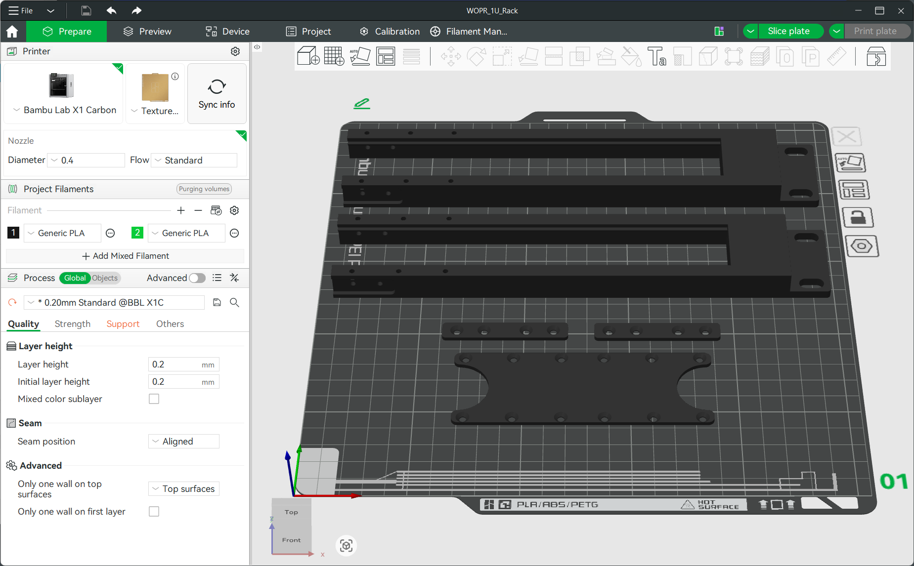
The plate with all the 3D printed parts in Bambu Studio.
I downloaded and opened the print in Bambu Studio. The print is relatively simple. It uses a lot of supports and takes about 3.5 hours to print the entire plate. The biggest challenge is that it does extend almost all the way to the edges of the print area. Plate adhesion can be a problem near the fan on the left side of the Bambu X1C but the plate temperature can be increased and the fan speed decreased if it is a problem.
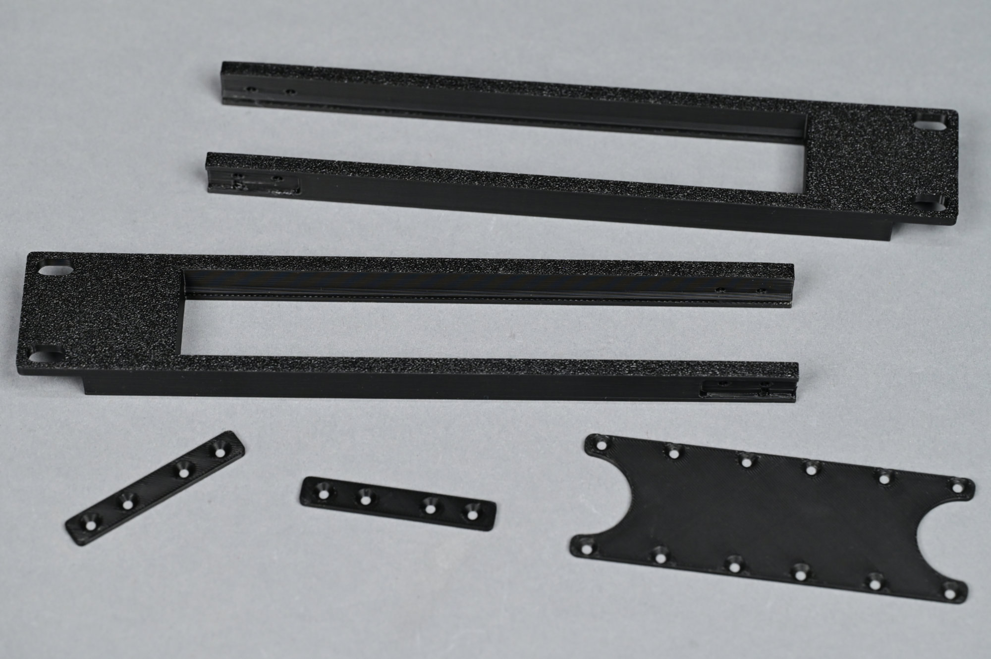
The completed 3D prints.
The 3D prints are shown in the photo above. They came out great!
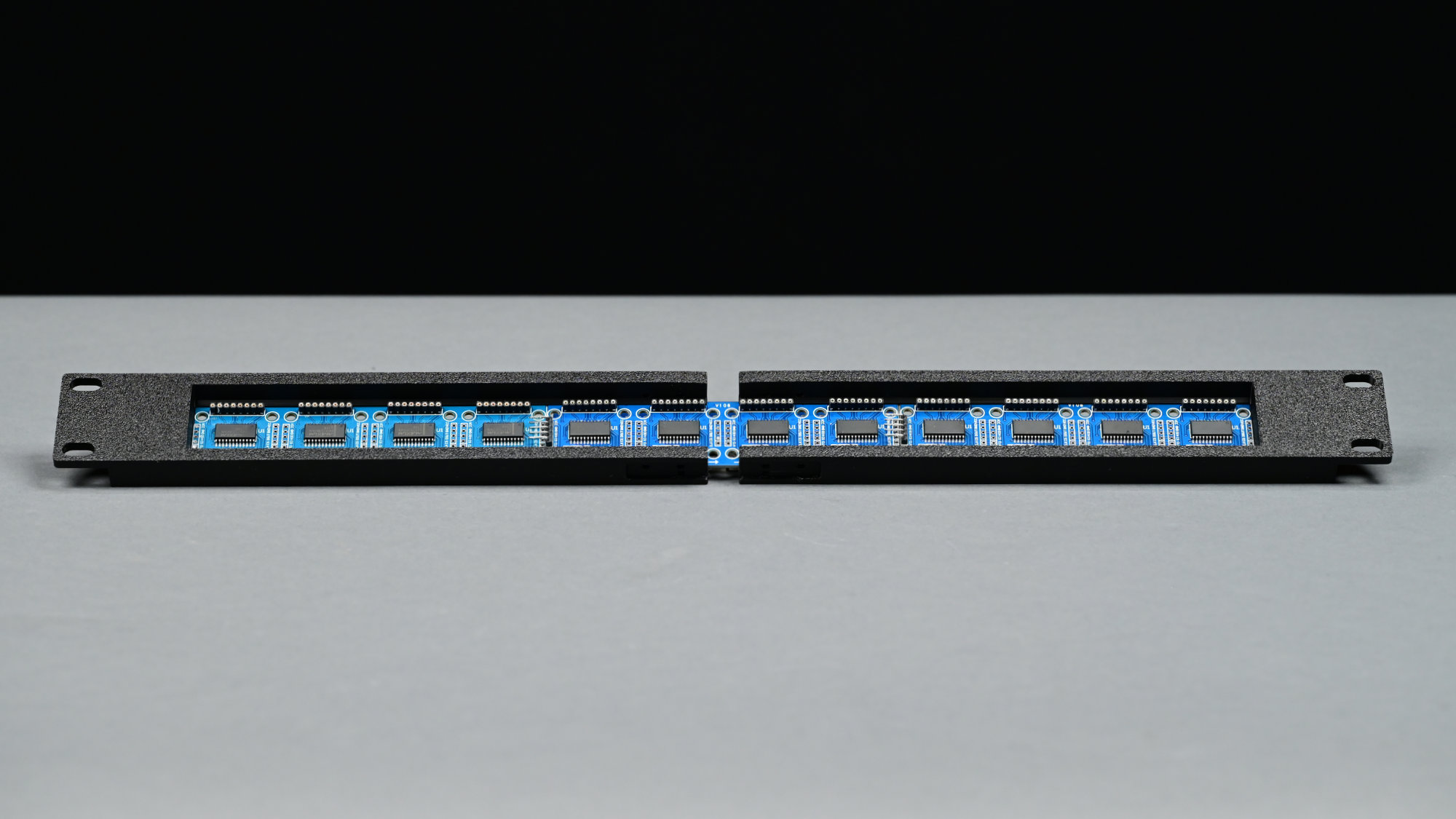
Whoops! This doesn’t look correct.
Even though the prints came out great, they were a bit short when I placed three of the MAX7219 4 x 8×8 LED modules into them. The gap is 12 mm. What went wrong? (The displays are missing in the above photo because I had already salvaged them for the final build before taking this photo.)
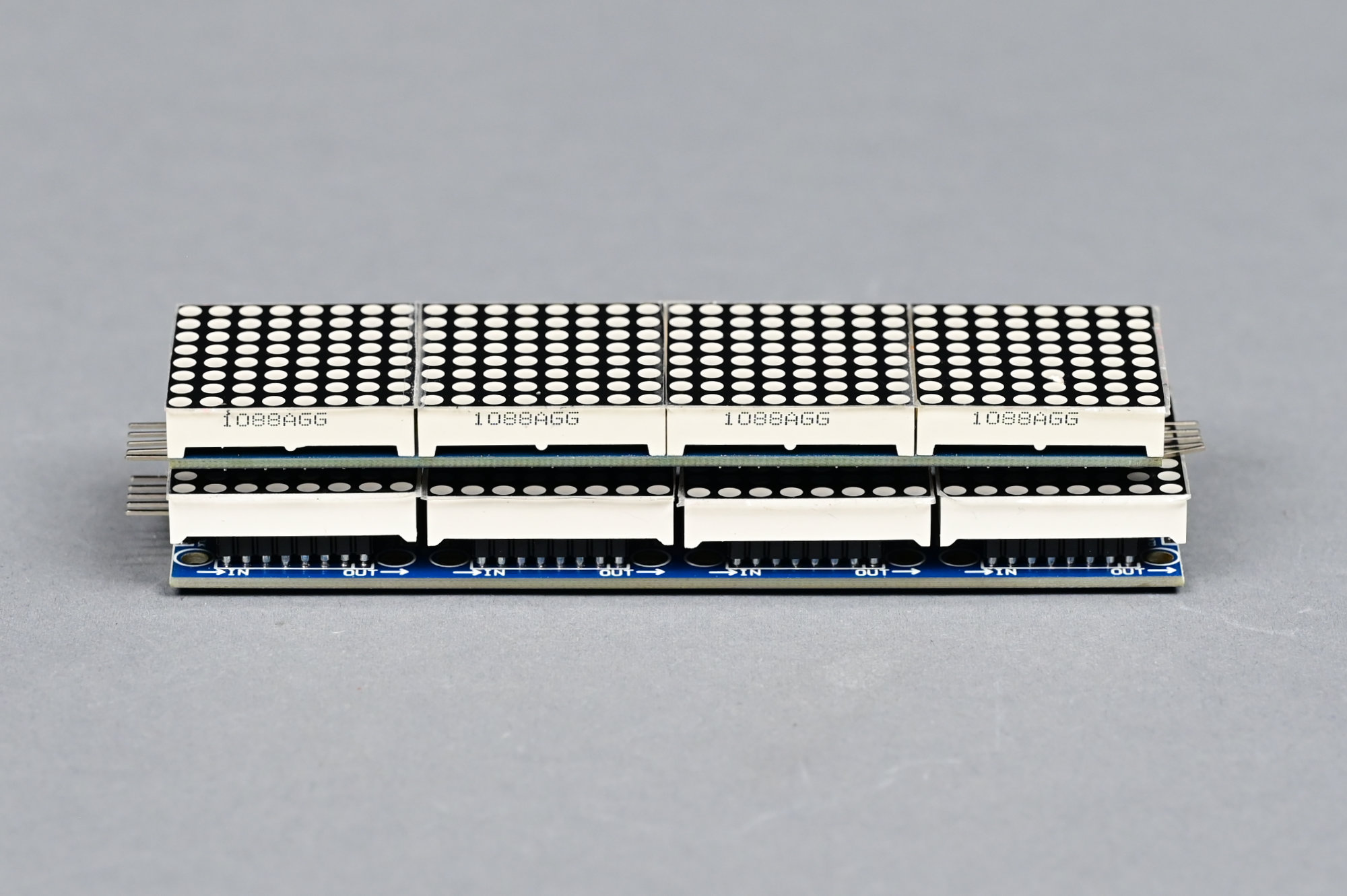
128 mm wide module on top. 132 mm wide module on bottom. Notice the gap between the displays on the bottom module.
After reading the comments on the original project on MakerWorld, I learned that the MAX7219 LED modules come in two widths: 128 mm and 132 mm. The 132 mm width modules have a gap of 1 mm between the displays. I did not want this gap so no problem, I’ll order a few of the 128 mm wide modules. That didn’t go as planned either.
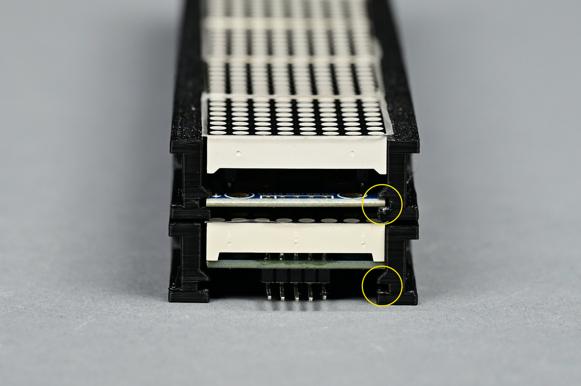
Top is a socketed LED module Bottom is an unsocketed LED module. The grooves in the 3D print capture the top module. The bottom module is just resting on the print and will fall out when stood up.
The first problem is many of the Amazon and AliExpress listings for the modules listed their dimensions as 128 mm but were actually 132 mm wide. The second problem is the modules that I found that were indeed 128 mm wide did not socket the LED displays and thus would not fit into the grooves in the 3D prints for the circuit board.
In the photo above the circuit board on the 132 mm wide module with sockets (top) fits in the grooves in the 3D print. On the 128 mm wide module without sockets (bottom), the circuit board can only sit above the slot and will fall out when the module is moved. The right slot is circled in yellow on each unit.
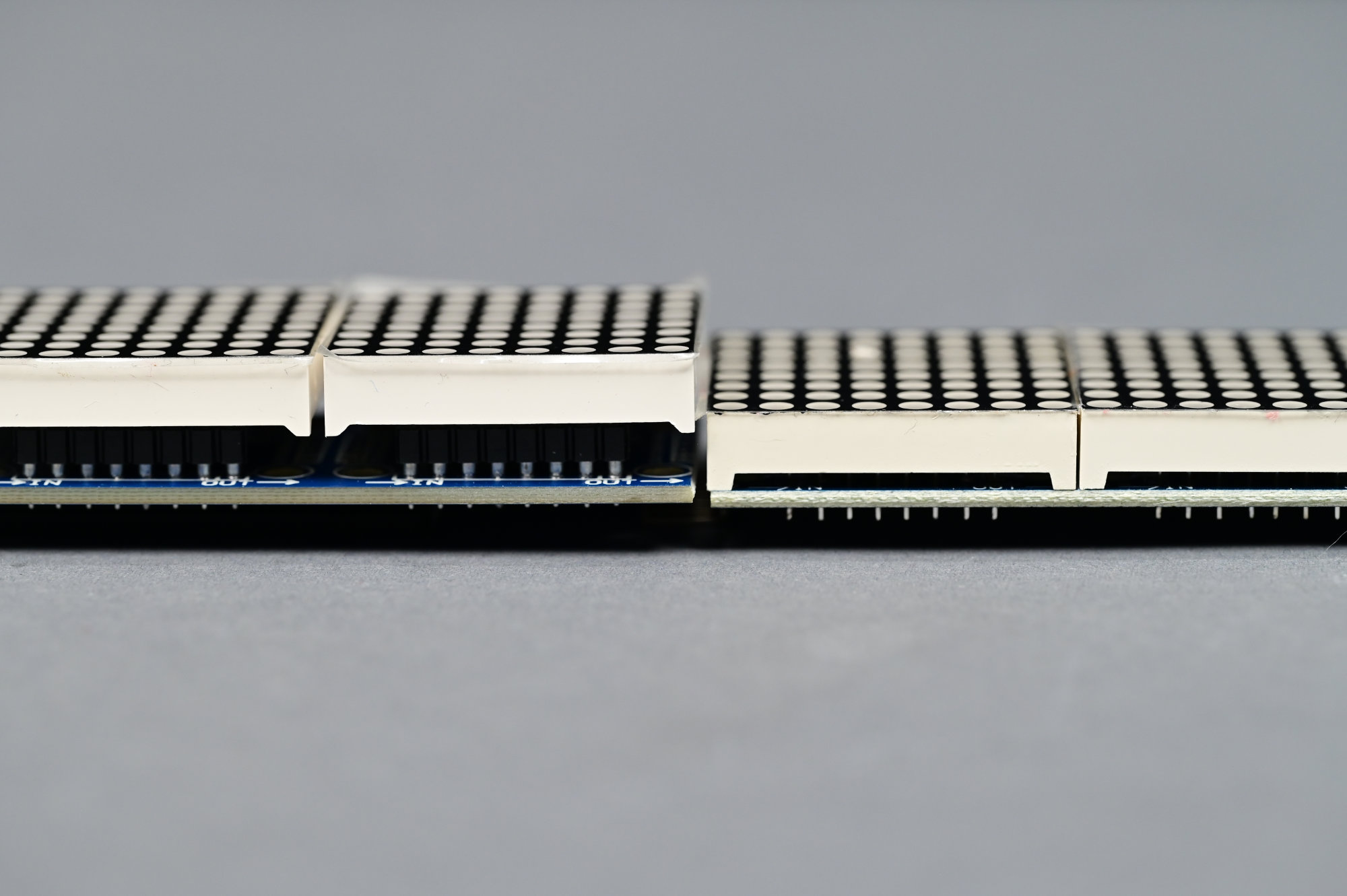
132 mm socketed module on left. 128 mm unsocketed module on right. The gap between the PCB and the LED display caused by the socket is crucial for the module to fit into and stay in the 3D print.
Turns out, the gap between the display modules and the circuit boards is essential for the modules to slide into the groove on the 3D prints and this gap only exists on the modules that use sockets. In the photo above, the white legs on the displays on the module on the right block the circuit board from fitting into the grooves on the 3D print.
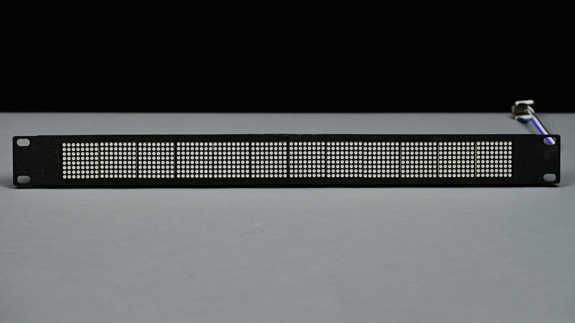
Not only is there a gap between each 8×8 display, the displays are not even aligned with each other.
Frustrated, I edited the STL to push each side out 6 mm to make room for the 132 mm wide modules and reprinted the files. This worked but I quickly tired of the 1 mm gap between the 8×8 displays and decided I could do better. Or could I?
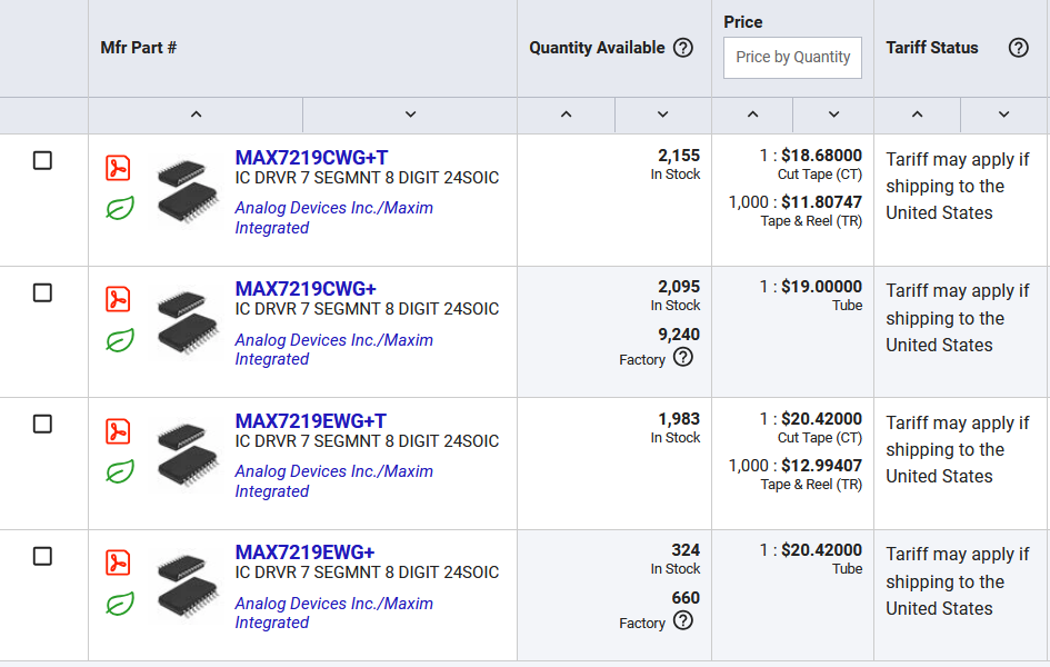
Ouch. $20 each. This is from Digikey but Mouser and others’ pricing is similar.
I figured the circuitry and board design were simple enough and I’d just build my own modules. They would be 128 mm wide with no gap between each display. That lasted right up until I saw the pricing for MAX7219 parts from reputable distributors. These parts are almost $20 each! I can get three boards with four parts each on them from Amazon or AliExpress for less than the cost of one new part from a reputable distributor!
The Plan
I formulated a new plan:
- I’d build a test board that was 32 mm x 32 mm. Four of them would equal a 128 mm wide module.
- I’d use sockets on my boards.
- I’d harvest both the displays and MAX7219 chips from cheap modules ordered off Amazon.
- Once that worked, I’d step and repeat the 32 mm layout four times to make a 128 mm wide module with four displays and four MAX7219 chips.
- Finally, I’d build up three of the four wide modules to make a seamless, 384-mm wide, 8 x 96 display that fit in the original unmodified 3D prints.
The Single Display Board
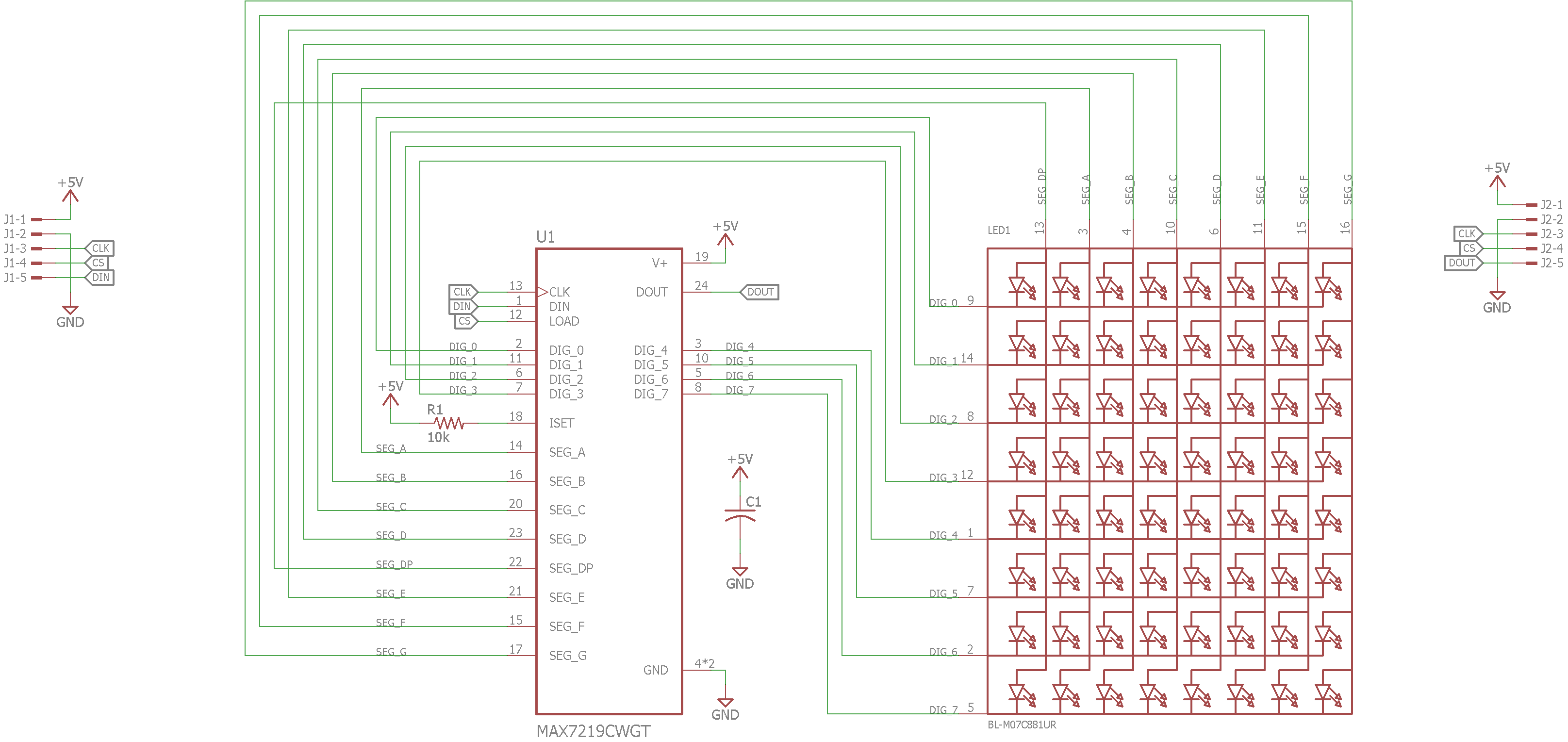
Schematic for a 32 x 32 mm, 8 x 8 pixel, single display module.
Just as there’s no definitive spec for these modules, there’s no definitive schematic either. I made my own schematic, shown above. The MAX7219’s segment pins are connected to the anodes of the LED matrix. The MAX7219’s digit pins are connected to the cathodes of the LED matrix. The only question was whether to put SEG_DP on the left of SEG_A or on the right after SEG_G. I figured it didn’t really matter since I could fix any row / column ordering issues in software later.
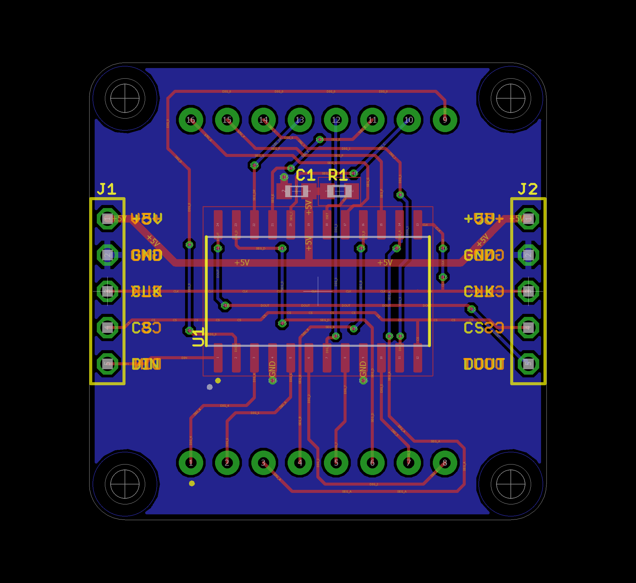
The PCB layout for the 32 x 32 mm, 8 x 8 pixel, single display module.
The layout of the board is shown above. It’s 32 mm square. Compared to the off-the-shelf boards, I rearranged the ordering of the input and output pins to simplify the layout. I also placed the input and output connectors 1.27 mm from the board edges with hopes I could daisy chain multiple boards together using jumper blocks rather than jumper cables.
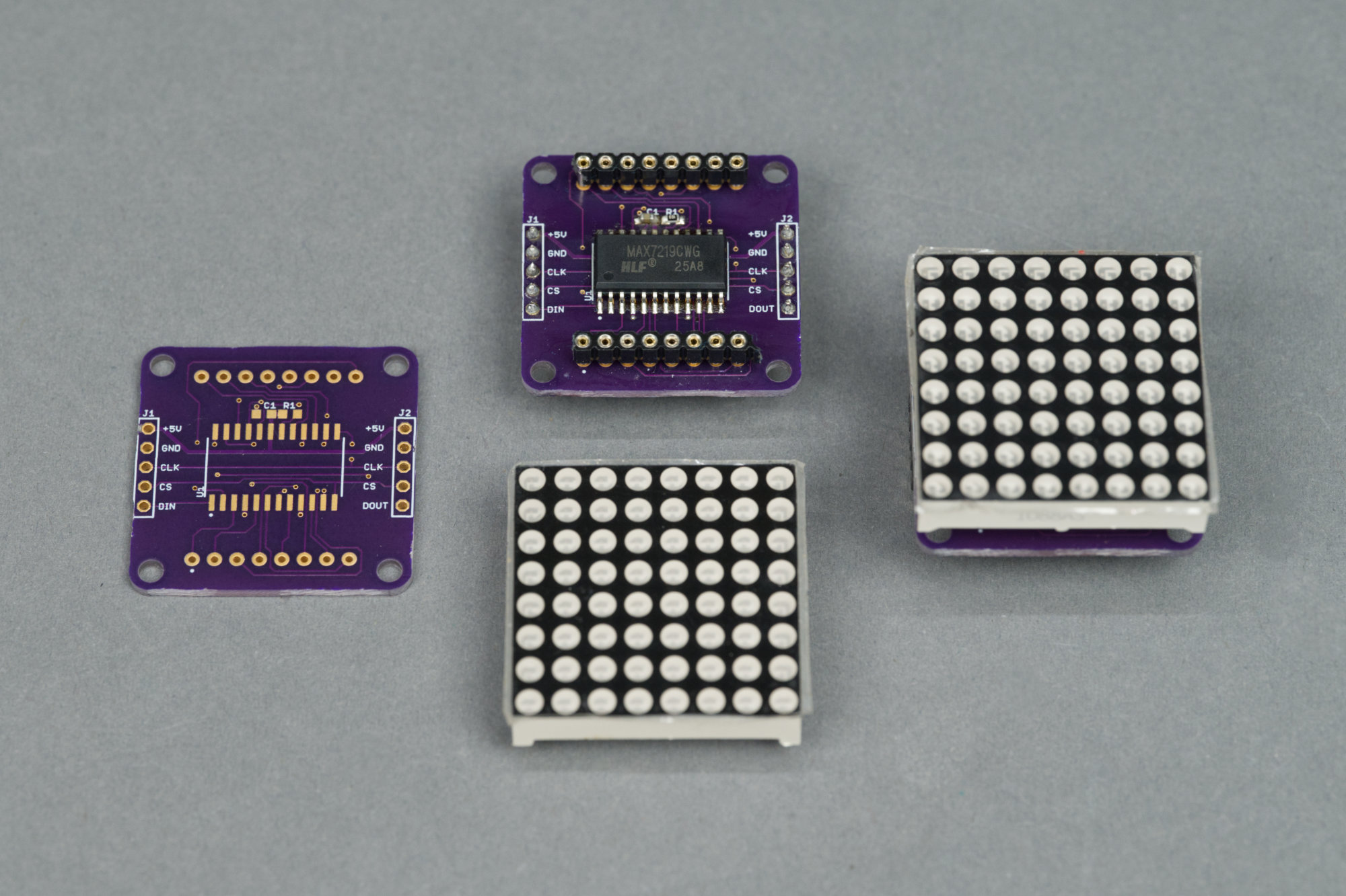
CW from left: unstuffed board, stuffed board, stuffed board with display, and just a display.
The photo above shows an unstuffed board, a stuffed board, and a stuffed board with the display inserted in the sockets, and an extra display. Time to bring up the boards and software.
Bring Up and Software Changes
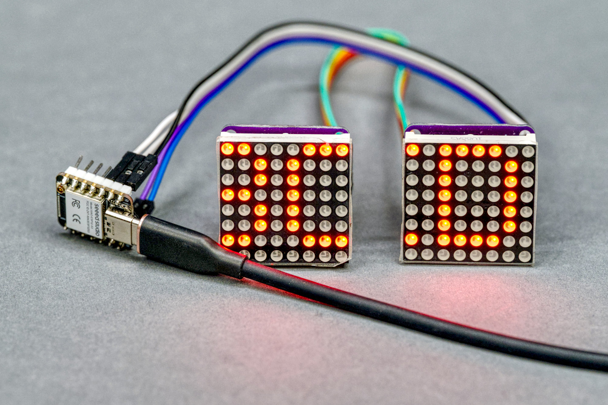
Bringing up the ESP32-S3 and the MD_MAX72xx examples on the single display modules.
The software for this project was written using the Arduino development environment and requires the MD_MAX72xx library. Most of the examples, as well as the original WOPR sketch, will run on my displays with only a minimum number of modifications.
The first change is the hardware type. This defaults to MD_MAX72XX::FC16_HW in the original WOPR sketch. I needed to change this to MD_MAX72XX::DR1CR1RR1_HW to use the sketch with my modules.
The second change is the number of devices. Since there are 12 displays, the MAX_DEVICES define needed to be change from 5 to 12.
The last change is to use the custom pin out on my controller board. I added some defines with the pin names and their GPIO numbers:
#define CLK_PIN   1
#define DATA_PIN  2
#define CS_PIN    3
Then I changed the global declaration of the MD_MAX72XX instance to use the initializer with all the pins instead of the simpler one that only has the chip select pin:
MD_MAX72XX mx(HARDWARE_TYPE, DATA_PIN, CLK_PIN, CS_PIN, MAX_DEVICES);
With these changes, any of the library examples or the WOPR sketch should run on my modules. The complete WOPR sketch with all the changes to run on my modules can be downloaded here.
Step and Repeat
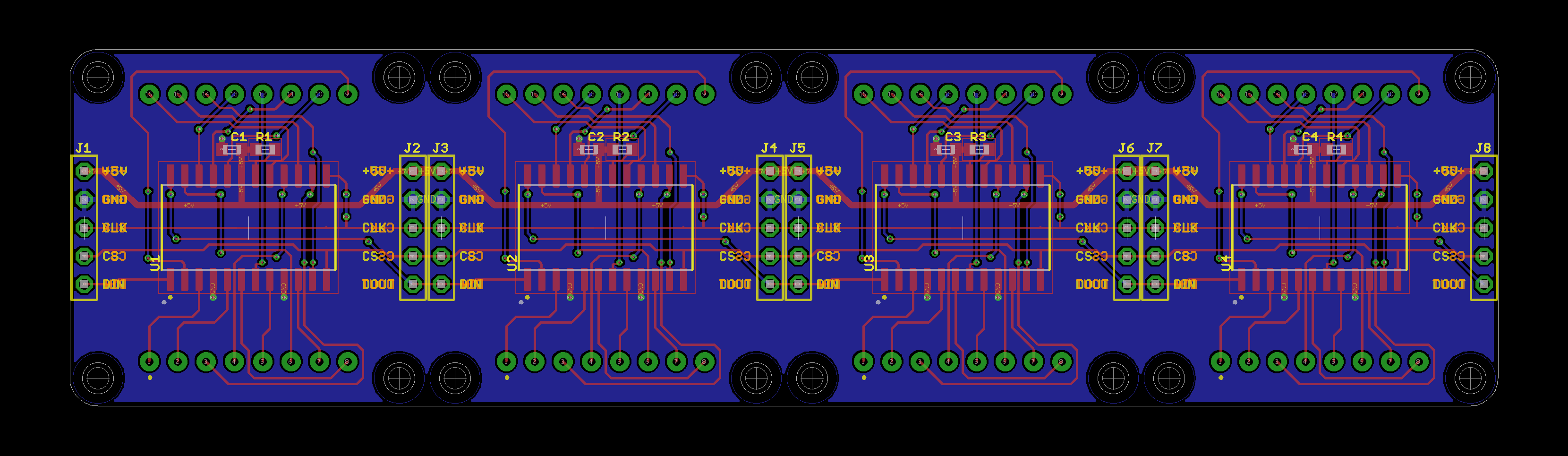
The PCB layout for a 32 x 128 mm, 8 x 32 pixel, quadruple display module.
With the single display boards working and, more importantly, working in series with each other, it was time to build a quadruple display version. I thought about creating a schematic with four copies of the single display schematic, but Eagle PCB doesn’t have a way to copy the layout of a group of components to a different group of components so I’d have to re-layout at least three of the display instances by hand.
The easiest (only?) way to do multiple copies of working layout in Eagle is to close the schematic and copy/paste the working layout then patch up any renamed nets that should be common like power and grounds, and in this case, the clock and chip select nets too. I ended up with the PCB layout in the image above. Of course, now there’s no corresponding schematic for this layout and Eagle does not have a way to create a schematic from a board.
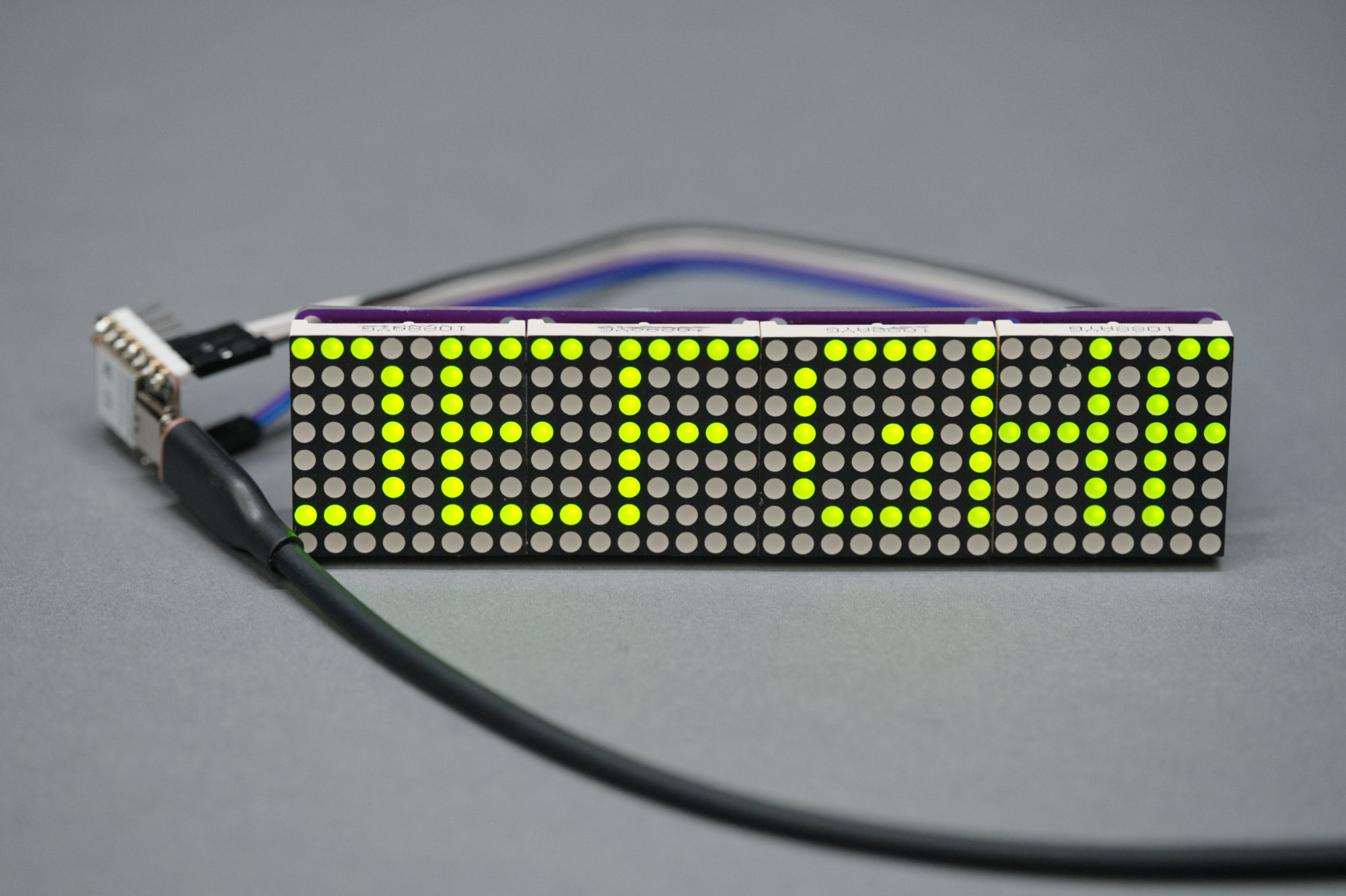
Bringing up my quadruple display module.
Once the boards were back from fab, I removed the displays and the MAX7219 chips from a bunch of cheap modules purchased on Amazon. I used ChipQuik’s SMD removal alloy and a soldering iron to remove the chips. Once removed, I used flux and solder wick to clean them up before soldering them to my boards.
I soldered the chips and some new sockets for the displays to my boards and inserted the displays in the sockets. I did my best to align the displays evenly. After assembling one board, I tested it by connecting it to an ESP32-S3 and getting the displays to work. Once one board worked, I finished the last two boards.
The Completed Units
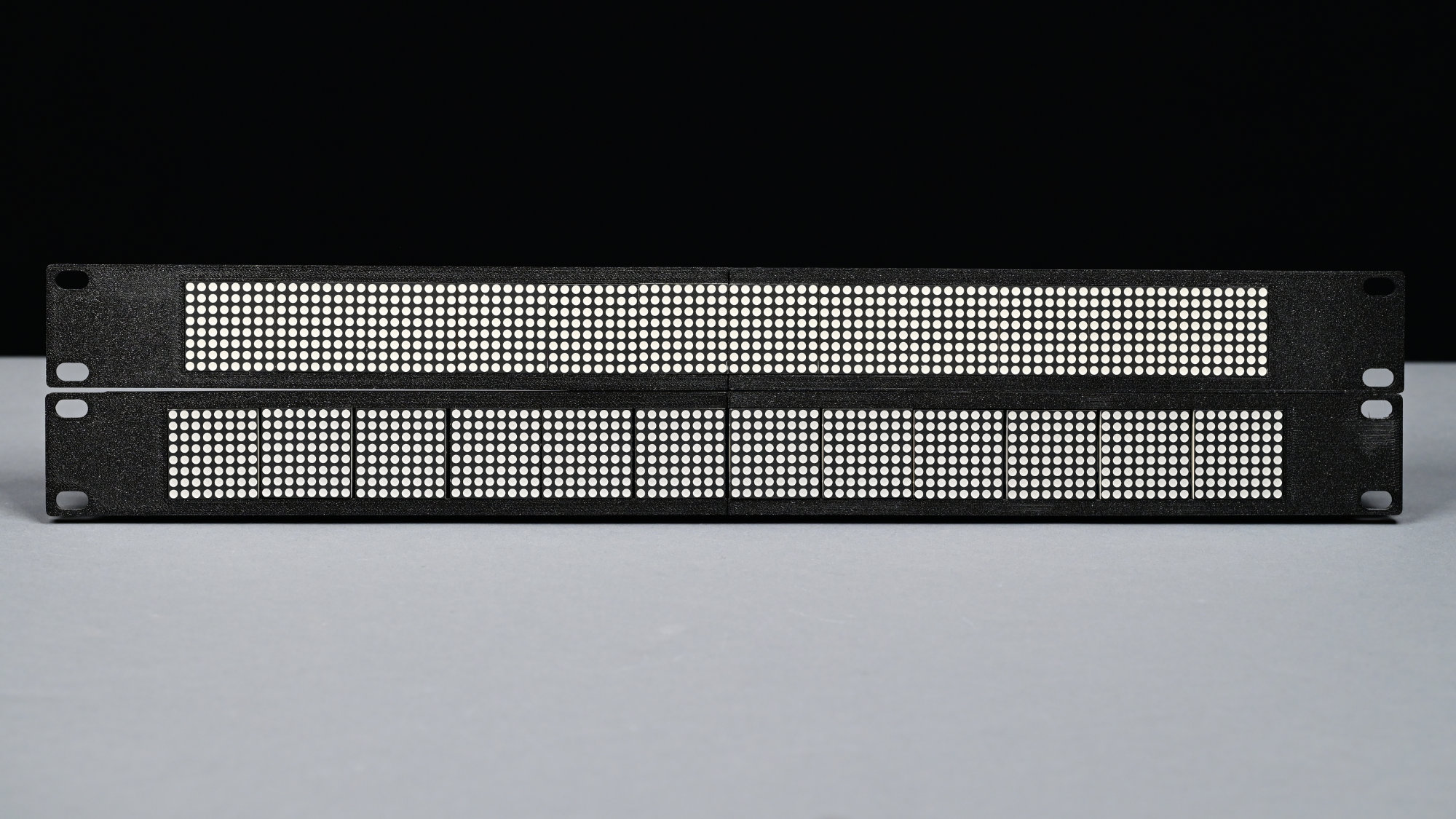
The completed rack mount units. The 128 mm no gap version on top and the 132 mm gap version on bottom.
The photo above shows the unit with my 128 mm wide boards (top) and the unit with the off-the-shelf 132 mm wide boards (bottom). The unit without the spacing between the 8×8 displays looks much better!
Bonus Content: Giving the ESP32-S3 Module a Home
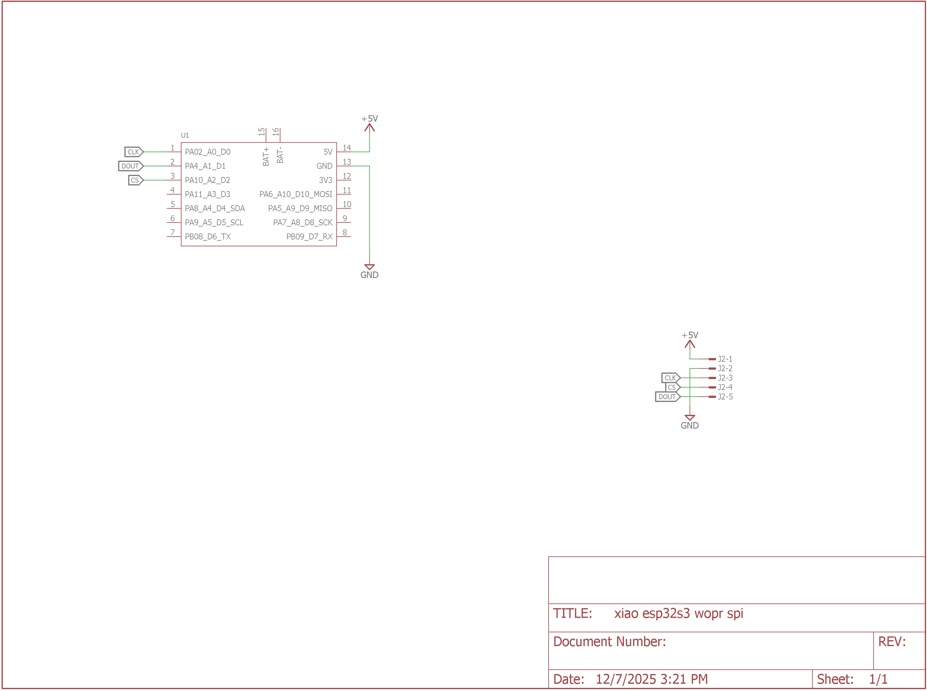
Controller board schematic.
The Seeed Studio XIAO ESP32-S3 module does not have mounting holes so I built a small board with mounting holes to hold the XIAO and break out the SPI pins. The XIAO solders directly to this board. The schematic of the controller board is shown above.
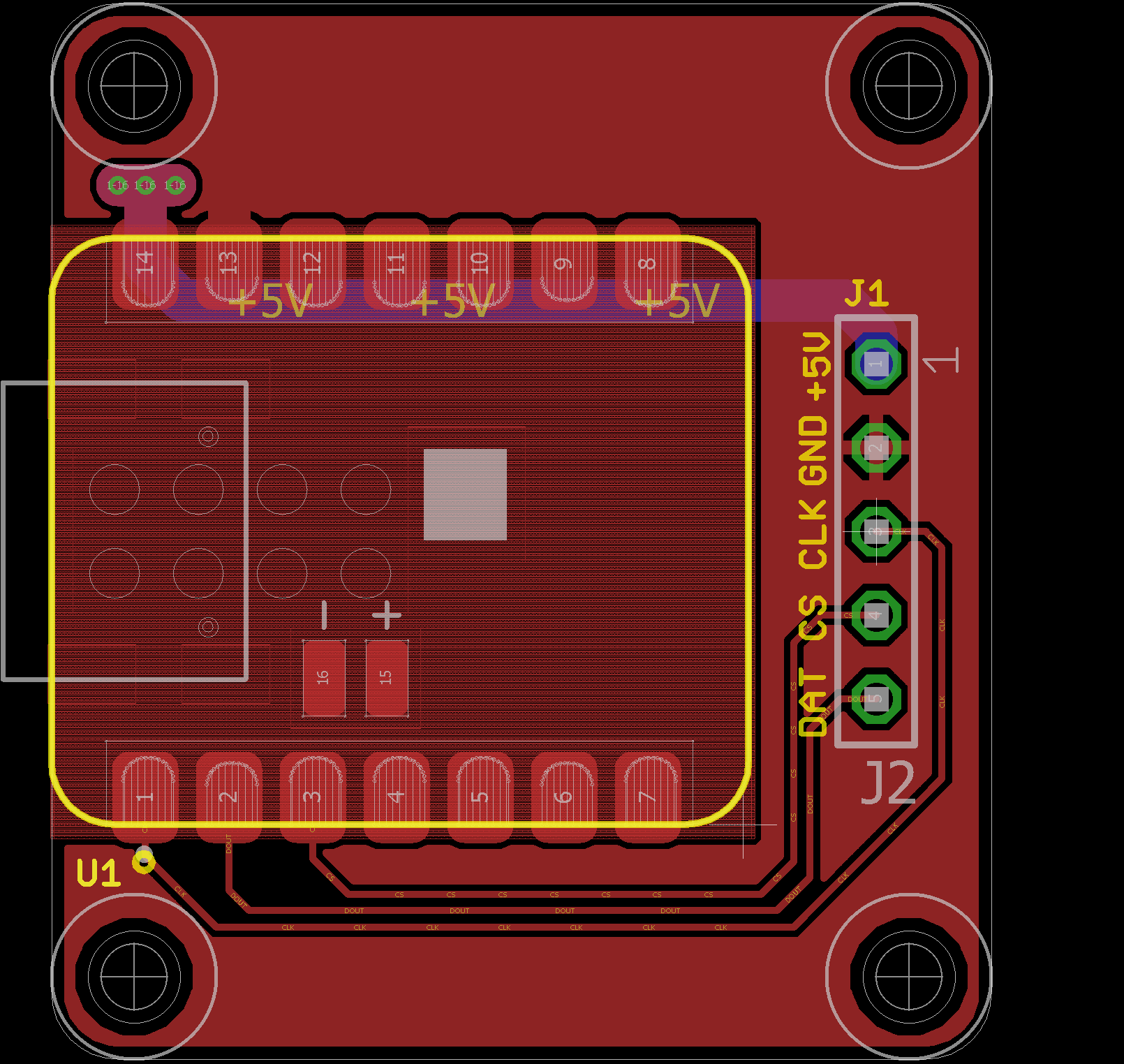
Controller board layout.
The layout of the controller board is shown above.
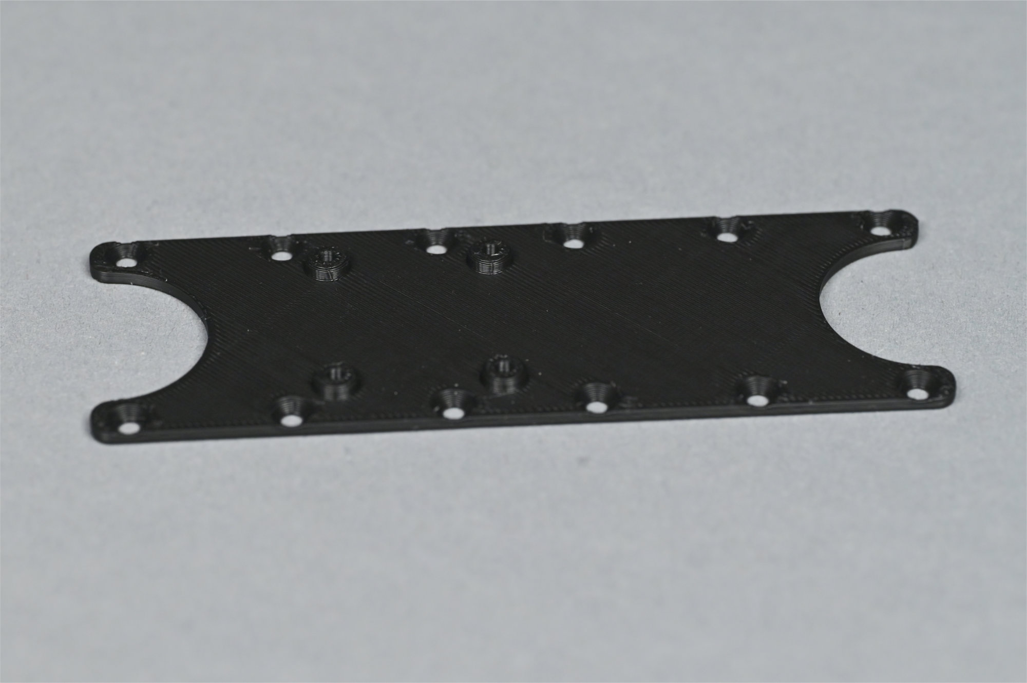
New back plate with mounts for the controller board.
I also added standoffs and mounting holes for the controller board to the large rear 3D-printed piece that joins the two halves of the rack mount together.
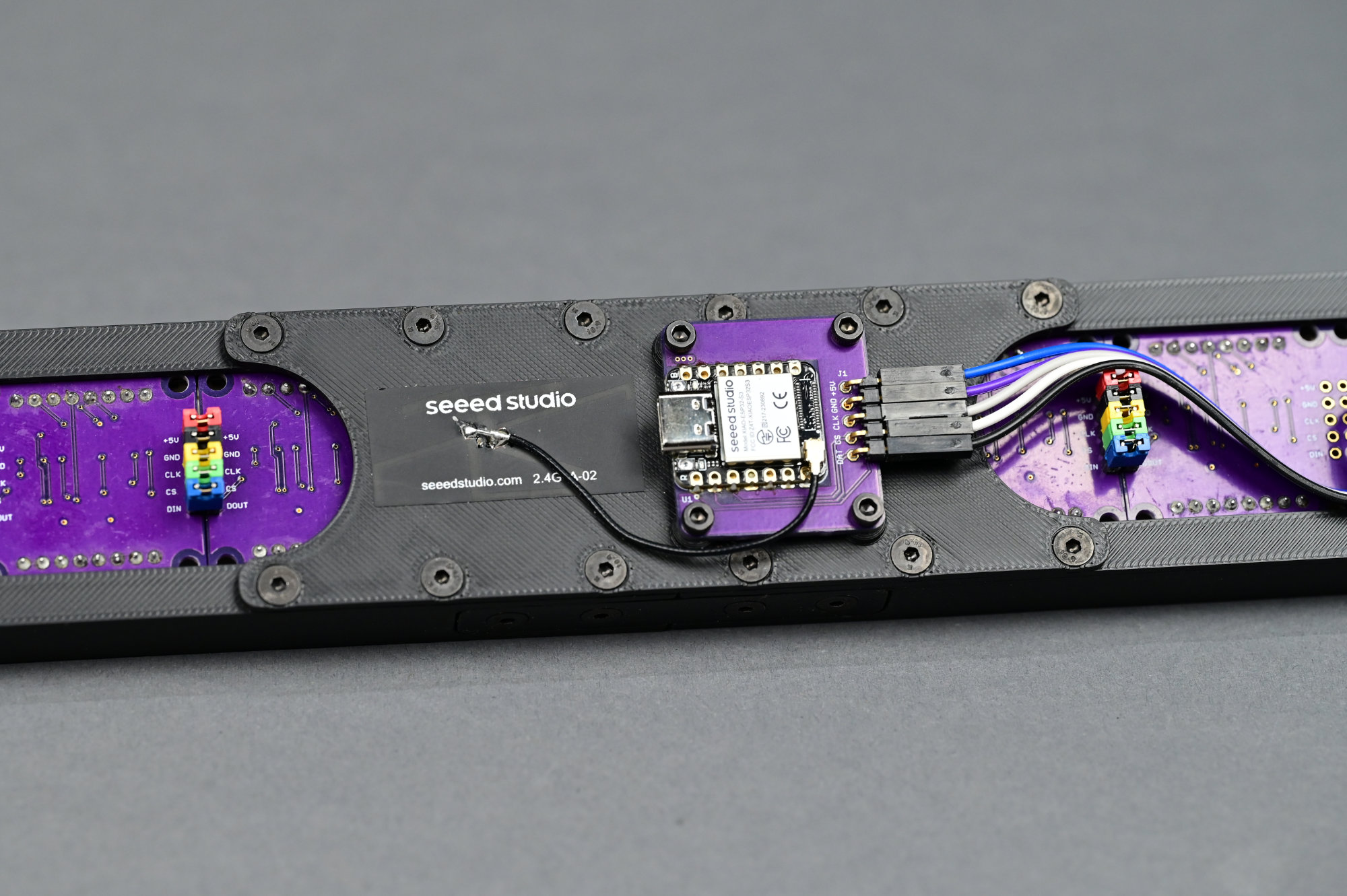
The controller board mounted to the back plate on the completed unit.
This allows the controller board to be mounted to the completed rack mount display rather than be left dangling off the back of the unit.
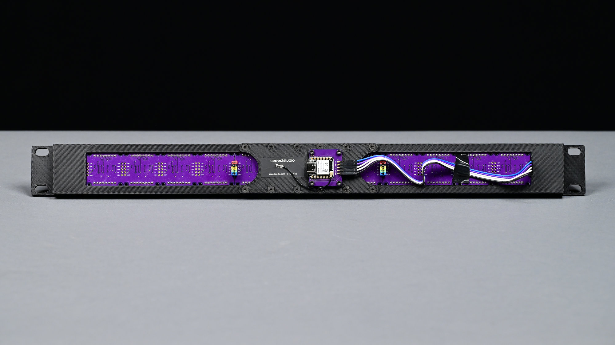
Rear photo of the completed unit.
Neat and tidy and self-contained!
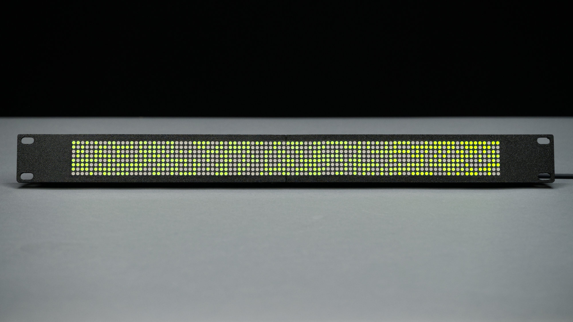
The WOPR LED rack mount filler panel lit up!
Useful Products
The list below contains links to some of the products I used in this project.
- Socket Pin Header Strips for Displays (Amazon, affiliate link *)
- Display Modules for Scavenging Displays and Chips (Amazon, affiliate link *)
- M3 x 5 mm Black Flat Head Hex Socket Cap Screws (Amazon, affiliate link *)
- ChipQuik SMD Removal Kit (ChipQuik, non-affiliate link)
- ChipQuik Solder Wick (ChipQuik, non-affiliate link)
* If items are purchased using the Amazon affiliate links, I will earn a small commission on their purchase.
Design Files
- Single Display Module
- Quad Display Module
- Controller Board
- Modified WOPR Arduino Sketch INO File
- Modified Rear Joiner Piece 3MF File
- Original Files
Late Update: The W.O.P.R. J.R.!
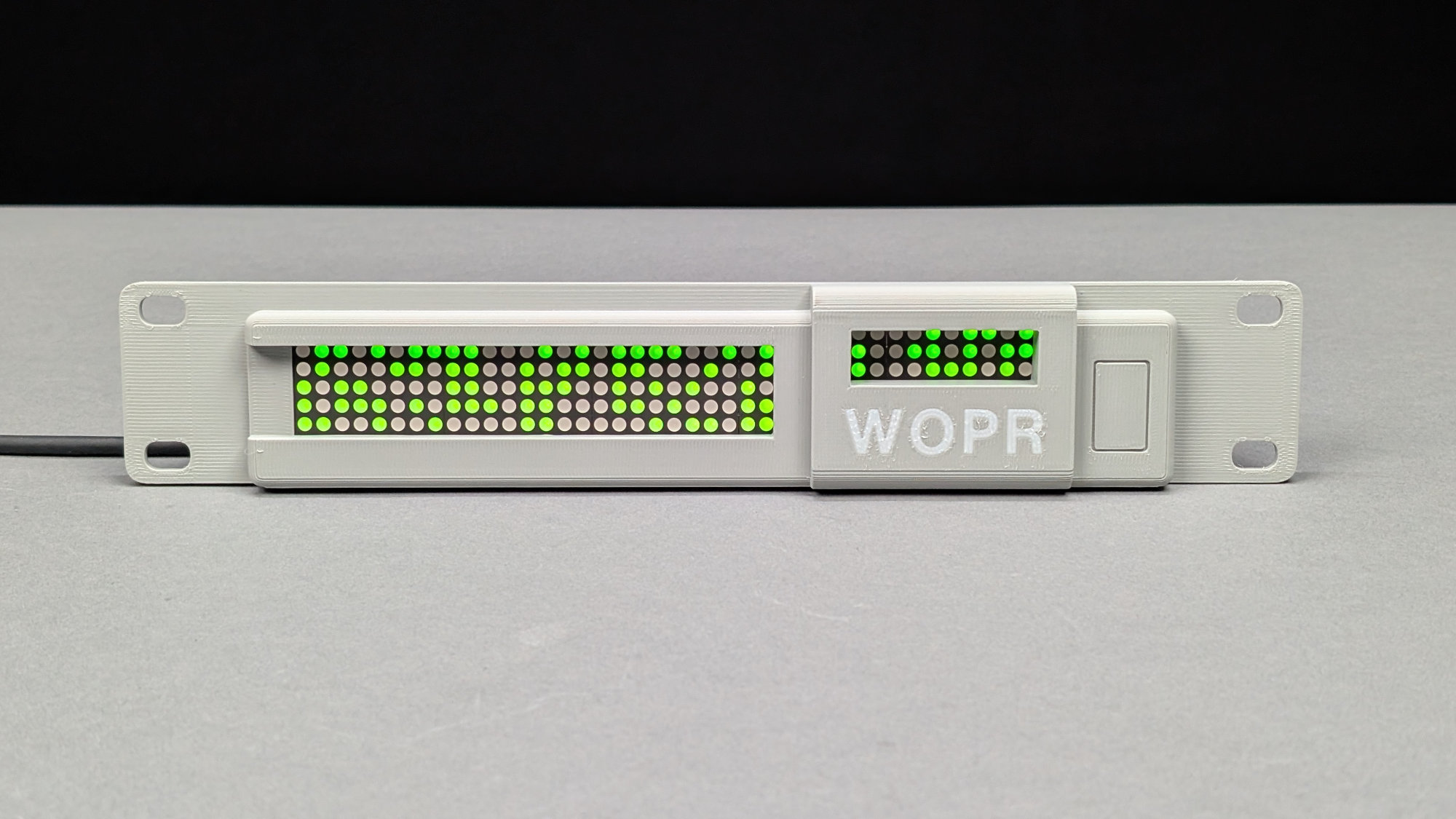
The completed WOPR Jr!
Another W.O.P.R.-related project on MakerWorld that caught my eye was a 10-inch rackmount version by a different designer. This one is great interpretation of the original W.O.P.R. computer from the movie. It uses the same modules that I designed for the larger 19-inch rackmount WOPR, but fits the popular 10-inch mini home lab rack form factor.
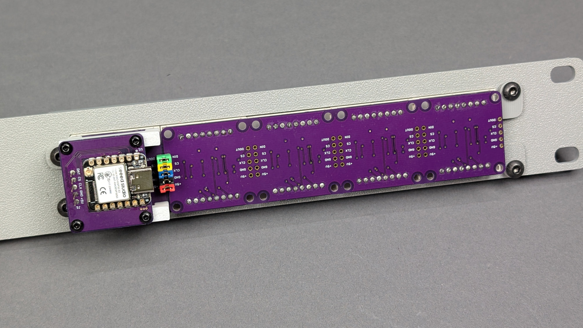
This project reuses the 32 mm and 128 mm wide module boards and the controller board.
This module requires five LED modules totaling 160 mm in width. I built the five modules from one 32 mm wide single module and one 128 mm wide quad module. They fit in a cavity in the back of the design and are held in place with two slats that slide through the modules which are secured using four M4 screws.
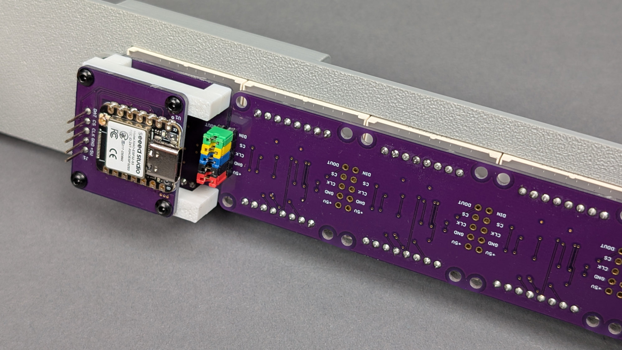
Close up of the controller board and its supporting 3D print.
The input of the single module is connected to the output of my controller board. The output of the single module feeds the input of quad module using five jumpers. A 3D printed bracket keeps the controller board from coming disconnected from the rest of the unit.
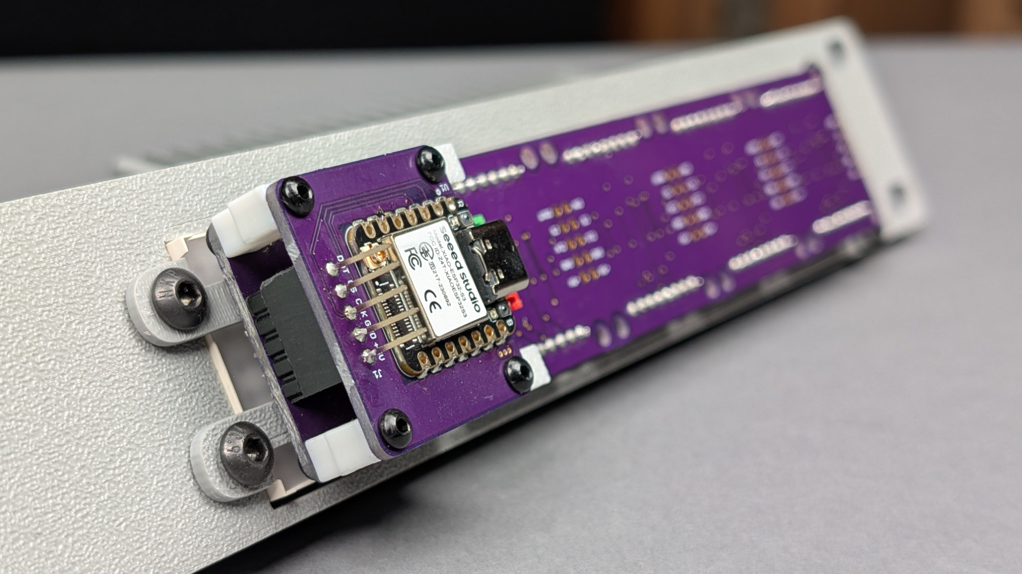
The controller board connects to the first display module board using a header socket mounted to the rear of the controller board.
The single module has a straight header. The straight header connects to a header socket on the back of the controller board. I used a long-tail header socket in case I want to connect a second LED board or a different LED board to this same controller board in the future.
W.O.P.R. J.R. Design Files
- WOPR 10 Inch Rack Mount 3D Prints on MakerWorld
- My board supports: wopr-jr-supports.3mf