RGB LED Panel Driver Tutorial
Project by Glen Akins, aka bikerglen, aka ktmglen
This project is © 2014 by Glen Akins. All rights reserved. It is released to the open source community under the terms of the GNU Public License (GPL) version three or higher.
Introduction
In this project, we interface a SparkFun or Adafruit 32x32 RGB LED panel to a BeagleBone Black board using the Xilinx Spartan 6 LX9 FPGA on the LogiBone FPGA board. The hardware for this project is relatively easy to construct—just 16 data signals connect the LED panel to the LogiBone FPGA board. The complexity of this project lies mostly in the RTL and software.
A demonstration of the project is available on YouTube.
A demonstration of the project expanded to six panels is also available on YouTube.
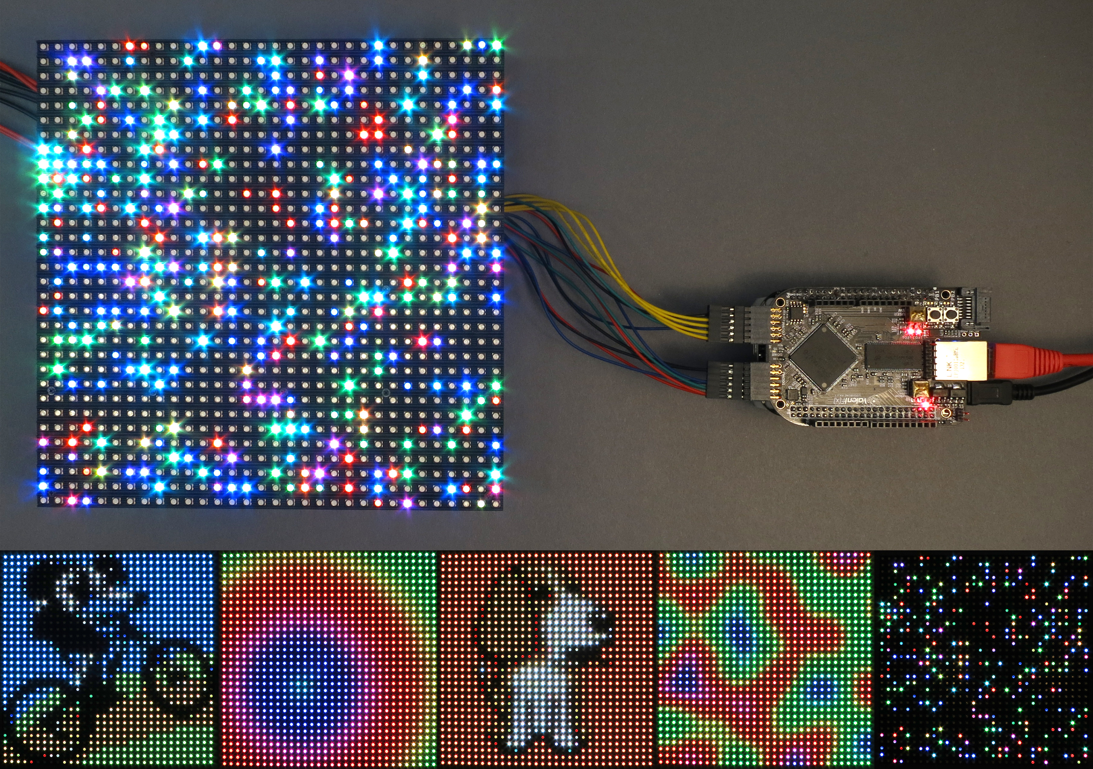
Figure 1. RGB LED panel with a random twinkling pattern connected to the LogiBone FPGA board and some other sample panel images.
Required Hardware
The following hardware items are required:
-
SparkFun or Adafruit 32x32 RGB LED panel
This panel contains 1024 RGB LEDs arranged in a 32x32 matrix. The columns are driven using multiple sets of shift registers and the rows are driven, two rows at a time, using a 4-bit address decoder. The panel is driven at 1/16th duty cycle and must be continuously refreshed to display an image. -
BeagleBone Black CPU board w/ USB or +5VDC power supply
You’ll need a BeagleBone Black CPU board and a +5VDC power supply for it. You can either use a USB cable to power the board from your computer or a USB power adapter or use a separate +5VDC, 2.1mm I.D., center-positive AC adapter. -
LogiBone FPGA board
The FPGA board contains a Xilinx Spartan 6 LX9 FPGA. The FPGA contains 32 18kbit block RAMs. We’ll use two of the block RAMs as frame buffers to hold the RGB pixel values to be displayed on the panel. The two Digilent PMOD-compatible connectors will be used to connect to the LED panel. -
Jumper wires or PMOD-to-display adapter board to connect the FPGA to the display
Initially, I used male-to-female jumper wires to connect the panel. This allowed me to connect the LogiBone FPGA board directly to the LED display panel without using the ribbon cable included with the display. If you only have male-to-male jumper wires, you’ll need to use the 16-position ribbon cable included with the display as an adapter to connect to the male pins on the display end of the jumper wires.
A much cleaner, long-term solution is to use this board and the 16-position ribbon cable included with the LED panel to make the connection from the LogiBone FPGA board to the display’s input connector. I also used precrimped terminal wires and housings to connect the FPGA and panel together. I didn’t like this solution because the precrimped terminal wires, when installed in a 2x8 housing connector, required too much force to insert onto and remove from the display’s data connector. -
+3.3V power supply, 2.0A nominal, 4.0A peak
During normal operation, the display will draw at most about 2A of current. If you “stall” the refresh with an all-white pattern displayed, the two rows that are lit will draw about 3.8A. A small 3.3V, 3.0A desktop power supply such as this one from Mouser will be sufficient during normal operation. You will need to supply your own IEC60320 C13 power cord to use with this adapter.
These panels can also be run from +5V instead of 3.3V. You will get brighter greens, brighter blues, and less-red whites if driven from +5V instead of +3.3V. You'll also pull about 15% more current and use about 65% more power at +5V instead of +3.3V. If you use a +5V supply, be extra careful not to accidently connect the LogiBone FPGA board to the display’s output connector. -
Female DC barrel jack adapter (optional)
A female DC barrel jack adapter will make connecting the panel to the power supply much easier. If you don’t have an adapter, you can always cut, splice, solder, and heat shrink the connections between the power supply and led panel.
Required Software
- Stock ValentFX LogiBone Ubuntu build w/ the LogiBone logibone_<revision>_dm.ko kernel module and logi_loader
Download and follow the instructions here to install the default LogiBone Ubuntu image on an SD card. - Xilinx ISE WebPack Software
If you want to build the FPGA bit file yourself or customize the Verilog to drive more panels or add other custom functionality (such as a coprocessor to help compute difficult pixel patterns), you’ll need to download and install the Xilinx ISE WebPack software. Instructions are here. If you only want to use the default FPGA bit file, you can skip installing the Xilinx ISE WebPack software. - Glen’s LED panel GIT repository
Finally, you’ll need to clone my GIT repository at http://github.com/bikerglen/beagle to your BeagleBone Black. This repository contains the Verilog source code for the FPGA, a prebuilt bit file, and C++ source code for displaying some demonstration patterns on the panel. Instructions for downloading or cloning and using the repository are presented later.
Theory of Operation
This system has three major components: the LED panel, the FPGA code, and the C++ code. Let’s examine each of these three major components in detail.
The LED Panel
LED Panel Hardware
The LED panel contains 1024 RGB LEDs arranged in a matrix of 32 rows and 32 columns. Each RGB LED contains separate red, green, and blue LED chips assembled together in a single package. The display is subdivided horizontally into two halves. The top half consists of 32 columns and 16 rows. The bottom half also consists of 32 columns and 16 rows.
The display’s columns are driven by one set of drivers and the display’s rows are driven by another set of drivers. To illuminate an LED, the drivers for both the column and the row for that LED must be turned on. To change the color of an LED, the red, green, and blue chips in each LED package are controlled individually and have their own column drivers. Figure 2 below is a schematic representation of the display’s column and row driver organization.
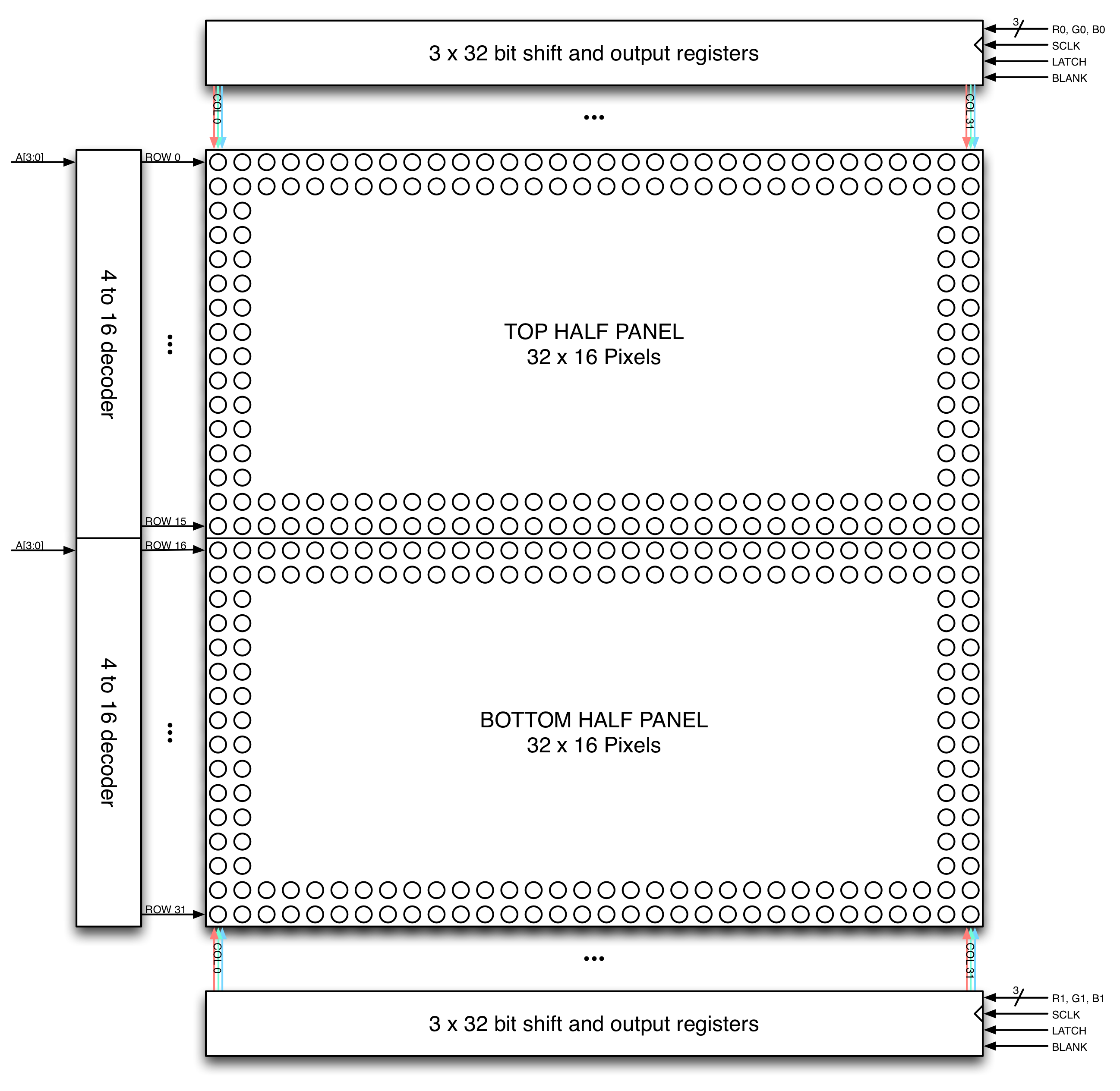
Figure 2. RGB LED panel column and row driver organization.
The panel contains six sets of column drivers; three for the top half of the display and three for the bottom. Each driver has 32 outputs. The three drivers for the top of the display drive the red, green, and blue chips in each of the 32 columns of LEDs in rows 0 to 15 of the panel. The three drivers for the bottom of the display drive the red, green, and blue chips in each of the 32 columns of LEDs in rows 16 to 31 of the panel.
Each of the drivers has a serial data input, a blanking input, a shift register, and a parallel output register as shown below in Figure 3. The data present on the serial data input is shifted into the shift register using the SCLK signal. After an entire row of data has been shifted in to the shift register, the LATCH signal is used to transfer the row of pixel data from the shift register into the parallel output register. If a bit in the output register is a ‘1’ and the blanking input is deasserted, the driver for that column will be enabled; otherwise, the driver will be turned off. Data is shifted from the right edge of the display to the left edge of the display. In other words, the first bit shifted in will be displayed on the left edge of the display and the last bit shifted in will be displayed on the right.
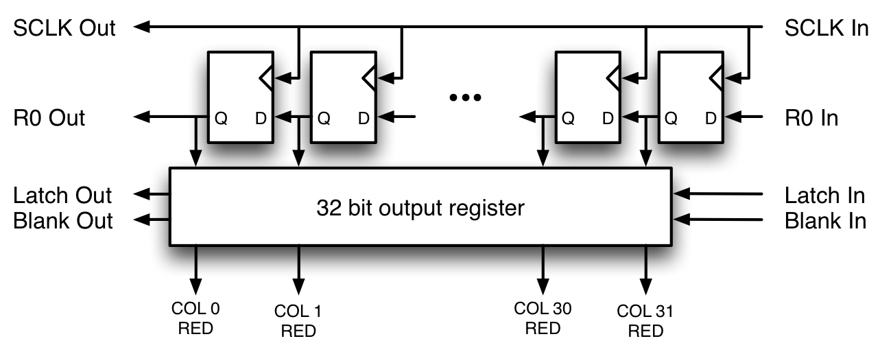
Figure 3. Column driver operation for the R0 data input and top-half red columns outputs. There are two more of these shift registers at the top of the display for the top-half green and blue columns and three more at the bottom for the bottom half red, green, and blue columns.
The red, green, and blue column drivers for the top half of the display are attached respectively to the R0, G0, and B0 data inputs. The red, green, and blue column drivers for the bottom half of the display are attached respectively to the R1, G1, and B1 data inputs. All six of the 32-bit drivers share common SCLK, LATCH, and BLANK signals.
The rows are driven using four address bits and an address decoder. The four-bit address input to the row drivers is decoded and the two row drivers corresponding to that address will be turned on. When A[3:0] is 0, rows 0 and 16 of the display are turned on. When A[3:0] is 1, rows 1 and 17 of the display are turned on. This pattern continues until A[3:0] is 15 and rows 15 and 31 are turned on.
In addition to the row and column logic and drivers, the display has a blanking input. This input is most likely connected to the column drivers. When the blanking signal is asserted, all of the pixels are turned off and the display will be black. When the blanking signal is deasserted, the addressed rows and columns will be driven and the corresponding pixels illuminated. To display an image without flickering and ghosting, all of these signals must be used and properly sequenced when driving the panel.
Driving the Panel
The display is multiplexed and has a 1/16th duty cycle. This means that no more than one row out of the 16 in the top half of the display and one row out of the 16 in the bottom half of the display are ever illuminated at once. Furthermore, an LED can only be on or off. If both the row and column for an LED are turned on, the LED will be illuminated; otherwise, the LED will be off.
To display an image, the entire LED panel must be scanned fast enough so that it appears to display a continuous image without flickering. To display different colors and different brightness levels, the brightness of the red, green, and blue LED chips within each LED package must be adjusted by varying the amount of time that each LED chip is on or off within a single refresh cycle.
The basic process used to refresh the display when using three bits-per-pixel color (one bit for red; one bit for green; and one bit for blue) is the following:
- Shift the pixel data for row 0 into the top column drivers and the pixel data for row 16 into the bottom column drivers using the R0, G0, B0, R1, G1, and B1 data inputs and the SCLK shift clock signal.
- Assert the blanking signal to blank the display.
- Set the address input to 0.
- Latch the contents of the column drivers‘ shift registers into the column drivers‘ output registers using the LATCH signal.
- Deassert the blanking signal to display rows 0 and 16.
- Wait some fixed amount of time.
- Repeat the process for each of the pairs of rows in the display.
- Repeat the entire process at least 100 to 200 times per second to prevent flicker.
The above process uses one bit per LED color. This will give you eight possible colors: black; the primary colors red, green, and blue; the secondary colors cyan, magenta, and yellow; and white.
To display more colors and brightness levels the above technique is modified to use binary coded modulation. In binary coded modulation, each pixel is controlled using more than a single bit per color per pixel. The amount of time each red, green, and blue LED chip is on is then varied proportionally to the pixel’s red, green, and blue values.
In binary coded modulation, the following process is performed to refresh the display:
- Shift bit zero of each pixel’s red, green, and blue values for rows 0 and 16 into the column drivers.
- Assert the blanking signal to blank the display.
- Set the address input to 0.
- Latch the contents of the column drivers‘ shift registers into the column drivers‘ output registers using the LATCH signal.
- Deassert the blanking signal to display rows 0 and 16.
- Wait some amount of time, N.
- Repeat the above process for the next higher order bit of color data in the same row. In step 6, wait two times the previous delay time. Repeat this process for each bit of color data, doubling the delay time after displaying each successive bit.
- Repeat the above process for each of the pairs of rows in the display.
- Repeat the entire process at least 100 to 200 times per second to prevent flicker.
Note that in actual implementations, the process of shifting the pixel data into the shift registers in Step 1 is usually done during the wait time in Step 6.
Global display dimming can be performed by varying the amount of time the blanking signal is asserted or deasserted within the wait time period, N. For example, asserting the blanking signal 25% early will result in a display with a brightness of 75% instead of 100%. Note that during global dimming, the wait time itself is not shortened or lengthened; only the blanking signal is modified to be asserted earlier than it normally would be.
The FPGA
The FPGA interfaces the C++ pattern generation software running on the BeagleBone Black CPU to the LED panel. The FPGA does the heavy lifting required to refresh the entire LED panel about 200 times per second. This leaves the BeagleBone Black CPU free to generate the patterns and perform other tasks.
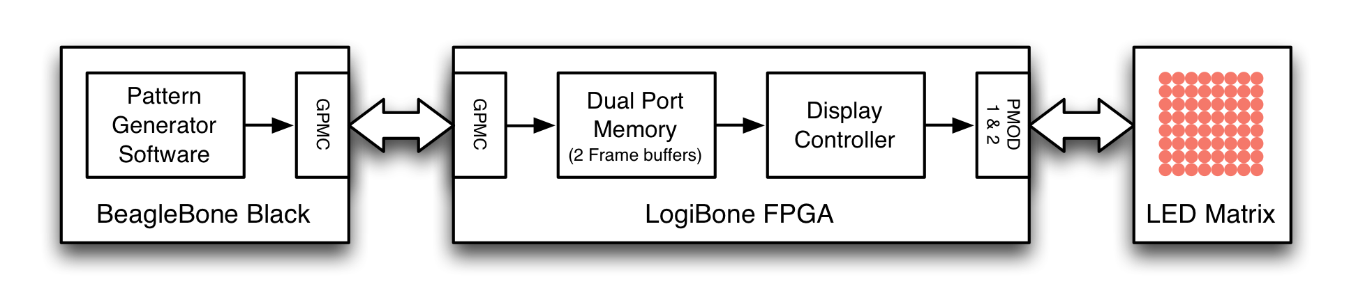
Figure 4. Block diagram of the system including a block diagram of the FPGA’s major functional blocks.
As shown in Figure 4 above, software running on the BeagleBone Black generates patterns. These patterns are fed to the FPGA on the LogiBone board using the TI SOC’s GPMC bus. These patterns are written to a dual-port memory that serves as a display buffer. Finally a display controller reads the patterns out of the dual port memory, shifts the data into the display, and enables the row drivers as needed to display the image. The entire process is repeated about 200 times per second and generates a 32 x 32 RGB image with 12-bit color without any interaction from the BeagleBone Blacks’ CPU.
GPMC Interface
The TI SOC has a programmable memory interface called the general-purpose memory controller (GPMC). This interface is extremely flexible. It can operate in both synchronous and asynchronous modes and the bus timing is programmable in 10ns increments. The GPMC bus will be used to transfer pixel data from the software on the BeagleBone Black to the FPGA on the LogiBone board.
In our system, the GPMC is configured to operate in its asynchronous, multiplexed address/data mode. In this mode, both the address and data buses are 16 bits wide. This permits an entire 12-bit pixel to be transferred from the CPU on the BBB to the FPGA on the LogiBone board in a single write operation. For more information on the GPMC’s asynchronous, multiplexed mode of operation, see sections 7.1.3.3.10.1.1 of the AM335x ARM® Cortex™-A8 Microprocessors Technical Reference Manual.
I’m using a slightly different circuit in the FPGA to interface to the GPMC bus than the stock LogiBone projects. It’s a bit slower than the stock VHDL circuit, but guarantees that each write from the CPU over the GPMC bus creates exactly one write strobe pulse to the register interface inside the FPGA. Because it’s slightly slower than the stock circuit, it requires modified bus timing and thus a custom device tree setup file. Figure 5 below shows the bus timing using the modified GPMC interface to perform a write to the FPGA. Figure 6 below shows the bus timing using the modified GPMC interface to perform a read from the FPGA.
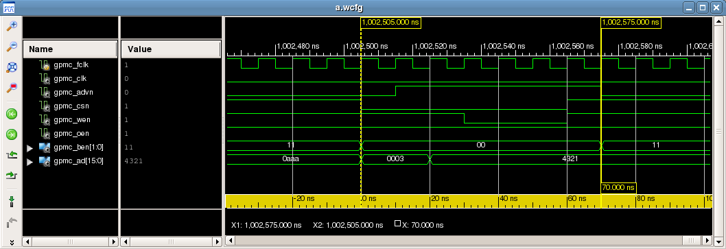
Figure 5. Simulation of a write to the GPMC target using the modified bus timings.
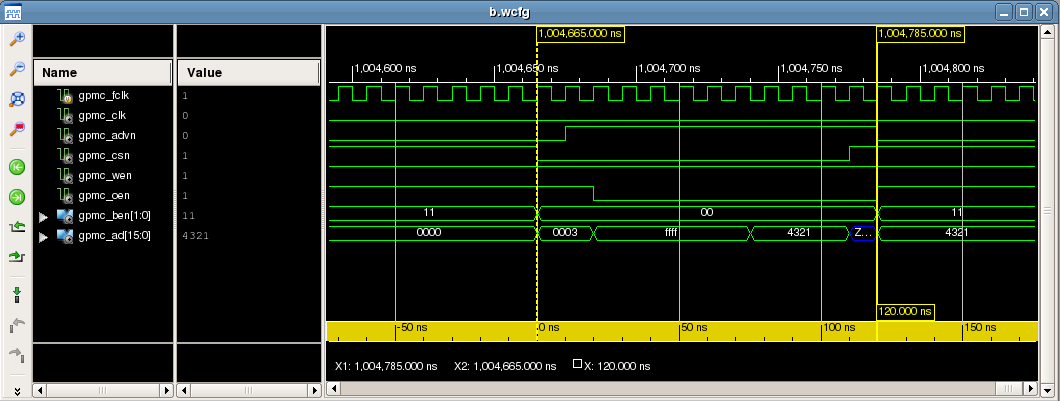
Figure 6. Simulation of a read from the GPMC target using the modified bus timings.
The read or write address is latched into a temporary holding register on the rising edge of the GPMC_ADVN signal and the write data is latached into its own temporary holding register on the falling edge of the GPMC_WEN signal. This requires using the GPMC_ADVN and an inverted version of the GPMC_WEN data signals as clocks. Technically, using data signals as clocks is gross. It’s actually so gross, the Xilinx tools will generate an error for this condition. But you can set an exception in the UCF file for the affected nets and force synthesis to continue. It would be much better to use the GPMC in its synchronous mode, but this technique is good enough for an FPGA until I have time to build a synchronous version of the interface, a synchronous GPMC bus model for simulation, and learn how to modify the device tree further.
In addition to latching the address and write data values into holding registers, the GPMC_CSN, GPMC_WEN, and GPMC_OEN controls signals are registered and brought into the FPGA’s 100MHz clock domain. Once in the FPGA’s clock domain, the WEN and OEN signals are gated with the CSN signal and edge detected to detect writes to the GPCM target and reads from the GPMC target. When a read or write is detected, the contents of the address and write data holding registers are captured into registers in the FPGA’s 100MHz clock domain.
The primary reason to slow down the GPMC bus versus the stock device tree setup file was to stretch the time that each of these control signals is low or high to at least 30ns to guarantee that the edges of the signals could be detected in the FPGA’s 100MHz clock domain. This also guaranteed that the address and data would be stable in their own holding registers before moving the contents of those registers into the address and data registers that are clocked in the FPGA’s 100MHz clock domain.
The outputs of the GPMC target are a bus that I’m calling the slow bus. The slow bus connects the GPMC target to the FPGA’s register interface. Figure 7 shows an example slow bus write operation. Figure 8 shows an example slow bus read operation.
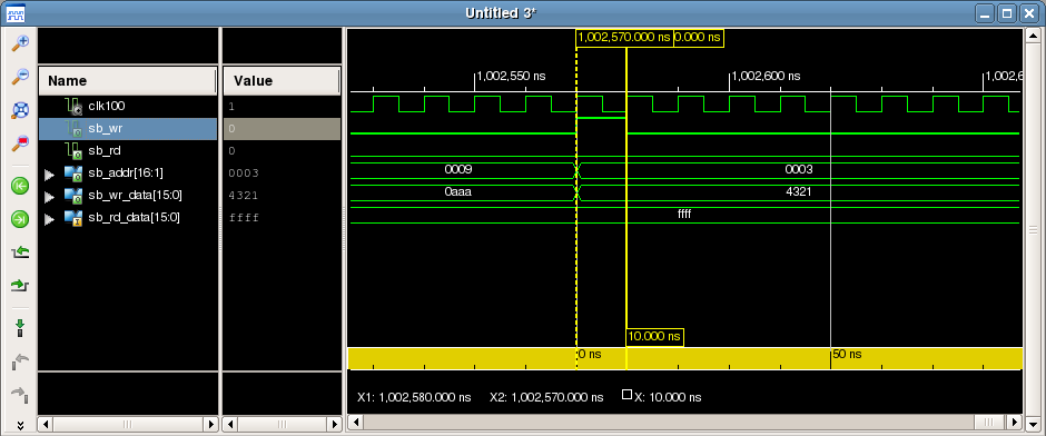
Figure 7. Simulation of a slow bus write.
sb_addr, sb_wr, and sb_wr_data will be valid for exactly a single 100MHz clock pulse every time a write occurs on the GPMC bus. When the register interface sees sb_wr asserted, it writes sb_wr_data into the register at sb_addr.
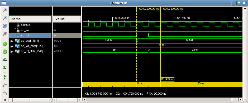
Figure 8. Simulation of a slow bus read.
sb_addr and sb_rd will be valid for exactly a single 100MHz clock pulse every time a read occurs on the GPMC bus. The register interface sees sb_rd asserted then must return the value of the register at the address sb_addr on the sb_rd_data bus on the very next clock cycle.
Register Interface
The register interface is implemented in the top level of the FPGA Verilog. The register interface defines the view the software has of the FPGA. Table 1 below lists the registers in the FPGA.
|
FPGA Address |
BBB SOC Address |
Name |
Description |
|
0x0000 |
0x0000 |
R/W Test Reg 1 |
Read / write test register. Write any value to this register. Reads return previously written value. |
|
0x0001 |
0x0002 |
R/W Test Reg 2 |
Read / write test register. Write any value to this register. Reads return previously written value. |
|
0x0002 |
0x0004 |
R/W Test Reg 3 |
Read / write test register. Write any value to this register. Reads return previously written value. |
|
0x0003 |
0x0006 |
R/W Test Reg 4 |
Read / write test register. Write any value to this register. Reads return previously written value. |
|
0x0004 |
0x0008 |
Read-Only Test Reg 1 |
Read-only test registers. Reads return hard-coded values. See RTL for returned values. |
|
0x0005 |
0x000a |
Read-Only Test Reg 2 |
Read-only test registers. Reads return hard-coded values. See RTL for returned values. |
|
0x0006 |
0x000c |
Read-Only Test Reg 3 |
Read-only test registers. Reads return hard-coded values. See RTL for returned values. |
|
0x0007 |
0x000e |
Read-Only Test Reg 4 |
Read-only test registers. Reads return hard-coded values. See RTL for returned values. |
|
0x0008 |
0x0010 |
Display Buffer Address Register |
Writes to this register set the display buffer address pointer. The display buffer address pointer points to the location in the display buffer memory that will be modified when a pixel value is written to the display buffer data register. See the display buffer section of this document for the arrangement of pixels in memory. |
|
0x0009 |
0x0012 |
Display Buffer Data Register |
Writing a pixel value to this register writes the pixel value to the display buffer at the address pointed to by the display buffer address pointer. After each write, the display buffer address pointer is incremented by one to point at the next pixel in the display buffer. |
|
0x000a |
0x0014 |
Display Buffer Select Register |
0 selects buffer 0 for display; 1 selects buffer 1 for display; Reads return which buffer is currently being displayed. |
Table 1. FPGA registers.
Display Buffers
The display buffers are implemented usinx Xilinx Block RAMs configured as dual-port memories with asynchronous read and write ports. The first RAM contains display buffers 0 and 1 for the top half of the display. The second RAM contains display buffers 0 and 1 for the bottom half of the display. Structuring the memories to contain half the display each permits the pixels in rows 0 to 15 to be read from memory on the exact same clock that the pixels in rows 16 to 31 are read from memory.
Display buffer 0 is located at address 0x0000. Display buffer 1 is located at address 0x0400. Each display buffer contains 1024 12-bit RGB values arranged as 32 rows of 32 columns. Within each display buffer, the top-left pixel is stored at offset 0, the bottom-right pixel is stored at offset 0x3ff. Bits 4 to 0 of the pixel offset are 0x00 for pixels in the leftmost column on the display; bits 4 to 0 of the pixel offset are 0x1F for pixels in the rightmost column.
Pixels are stored in the memory as 12-bit RGB values. These values are stored right-justiified. Bits 11 to 8 are the red pixel level, bits 7 to 4 are the green level, and bits 3 to 0 are the blue level.
Display Driver
The display driver reads pixel values from memory, shifts those values to the display, and cycles through the rows of the display as required to implement binary coded modulation as described in the theory of operation section of this document. The display driver is implemented as a state machine. Each state implements a step in the refresh process. When that step is complete, the state machine moves to the next step in the process.
Figure 9 below shows simulation waveforms for the control and data outputs for three rows worth of display data. The basic process is to blank the display, latch in the previously shifted data, update the row selects, unblank the display, shift in the next set of pixel data, and then wait for an update timer to expire. This is repeated four times for each row. If you examine the blanking output, you’ll notice that its low period doubles three times within the output period for each display row. This is the result of using binary coded modulation to vary the intensity of each pixel.
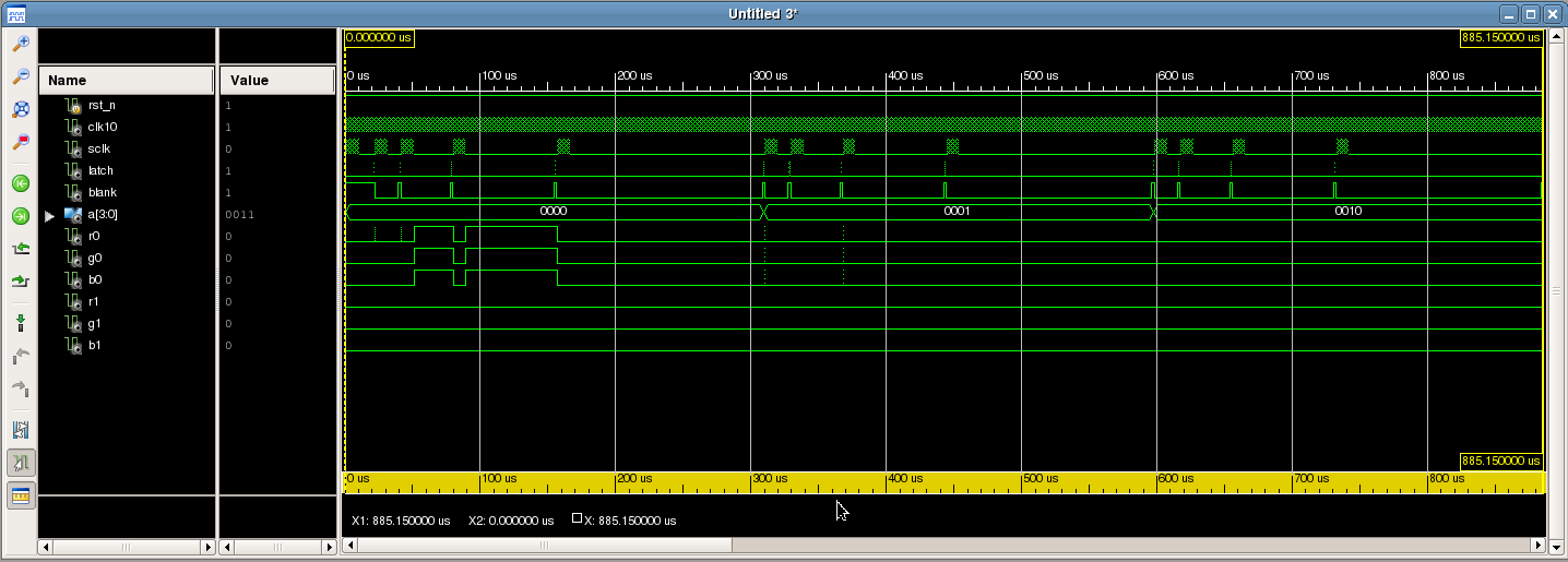
Figure 9. Simulation waveforms for the display data output connections.
The Software
The demonstration software uses the /dev/logibone_mem device to communicate with the FPGA. The driver for this device is part of the stock LogiBone Ubuntu image and its loadable kernel module is installed by the modified device tree setup shell script that’s included in the GitHub repository for the LED panel. (More on this subject in a later section.) This driver maps the registers in the FPGA to a portion of the BBB CPU’s address space using the GPMC. The GPMC normally maps memory into the CPU’s address space. Because our FPGA looks like a memory to the GPMC bus, its registers can be mapped into the CPU address space too. Pretty cool. No SPI, I2C, etc.; just fast parallel accesses between the CPU and the FPGA. This memory-mapped space can then be accessed by opening the /dev/logbone_mem device using the C library open function call and reads and writes to a register in the FPGA can be performed using the pread and pwrite C library function calls.
Figure 10 below is a block diagram of the demonstration software stack. In the demonstration software, main opens the /dev/logibone_mem device, fills the global buffer memory, gLevels, with all black, and then calls WriteLevels to write the global buffer to the display and clear the display. Once the display is cleared, the main function instantiates a pattern / animation subclass such as a radiating circle, perlin noise, or colorwash subclass. This subclass is derived from a generic pattern base class.
The generic pattern base class uses a constructor to set the height and width of the pattern to generate. Derived classes may add their own arguments to their own constructors. The base class also has two pure virtual member functions, init and next, that any derived classes must implement. The init function prepares a pattern to be displayed for the first time. It typically resets any state information back to the start of the pattern. The next function calculates the next frame of the pattern and writes that frame to the global gLevels buffer.
After main has instantiated the pattern subclass, it calls the subclass’s init funciton. Main then installs a timer that executes at 50Hz and goes to sleep. When the timer expires, a timer handler function is called. The timer handler function calls WriteLevels to write the previously computed frame in gLevels to the next available display buffer in the FPGA and makes that display buffer active. The writes to the FPGA display buffers are performed using the registers documented in the Register Interface section of this document.
After WriteLevels has completed, the timer handler function calls the pattern’s next member function. The next function generates the next frame in the animation, writes that frame to gLevels, and returns—without calling WriteLevels. The timer handler then sleeps until the next time the timer expires. By calling WriteLevels before calling next, the amount of time between displayed frames will not vary even if the amount of time that next takes to execute varies between frames.
In order for animations to run smoothly, the timer handler function must complete execution before the timer expires next. This means that each frame in the animation must take less than roughly 20ms to compute.
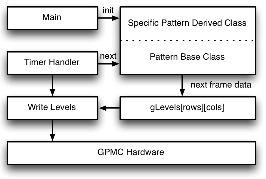
Figure 10. Block diagram of the demonstration software stack.
Connecting the Hardware
The display requires only a data connection to the LogiBone FPGA board and a power connection to a +3.3V power supply to operate. These connections are detailed in the sections below.
Display Data Connections
Figure 11 below lists the connections between the PMOD connectors and the display’s data input connector. You will need to make 16 connections total between the LogiBone board and the display panel. Thirteen of these are data connections; three of these are grounds. You can either use jumper wires or the PMOD-to-display adapter board. If you use jumper wires, the wiring will look something like Figure 12. With the adapter board, it will look something like Figure 13. Note that the PMOD connectors’ pins are numbered differently than double row headers are normally numbered.
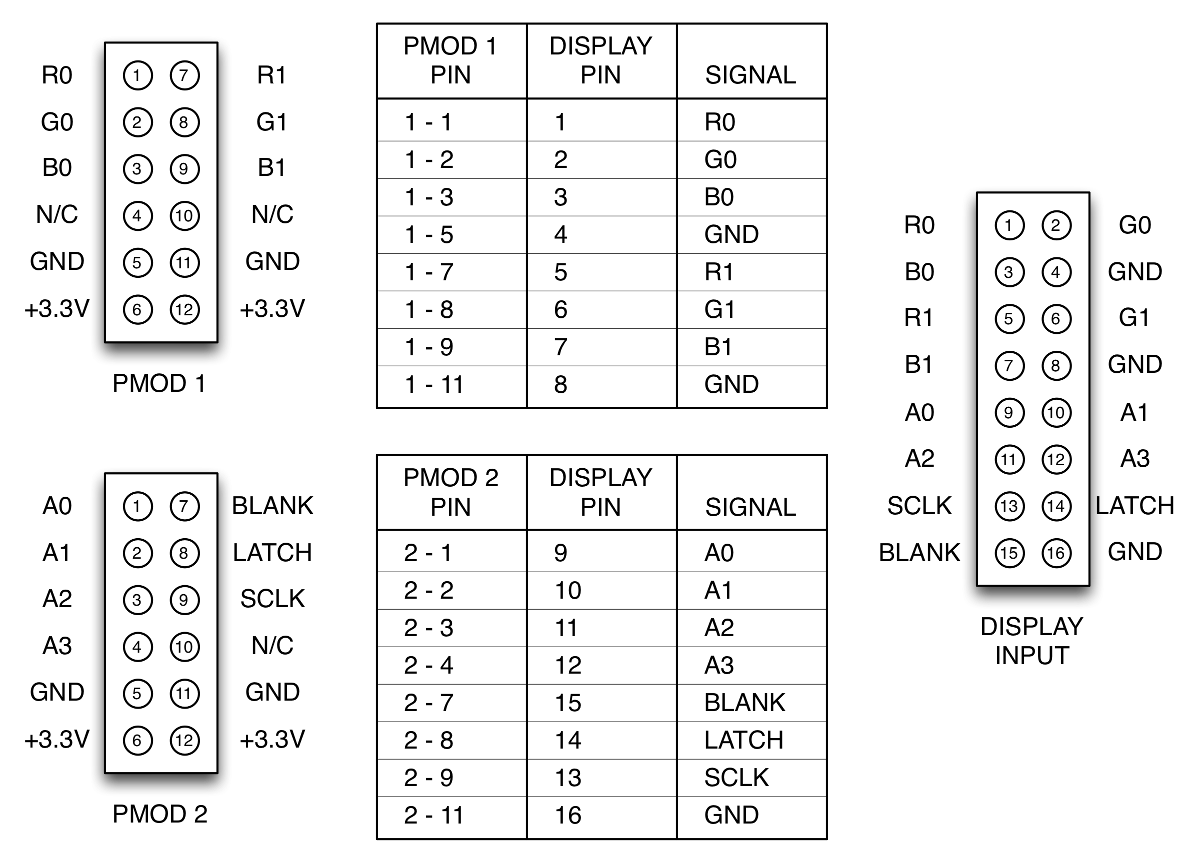
Figure 11. PMOD connector pin outs, connections between the PMOD connectors and the display input connector, and the display connector pin out.
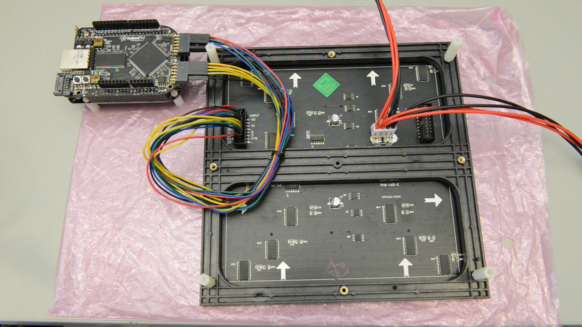
Figure 12. LogiBone FPGA board connected to RGB LED panel using jumper wires.
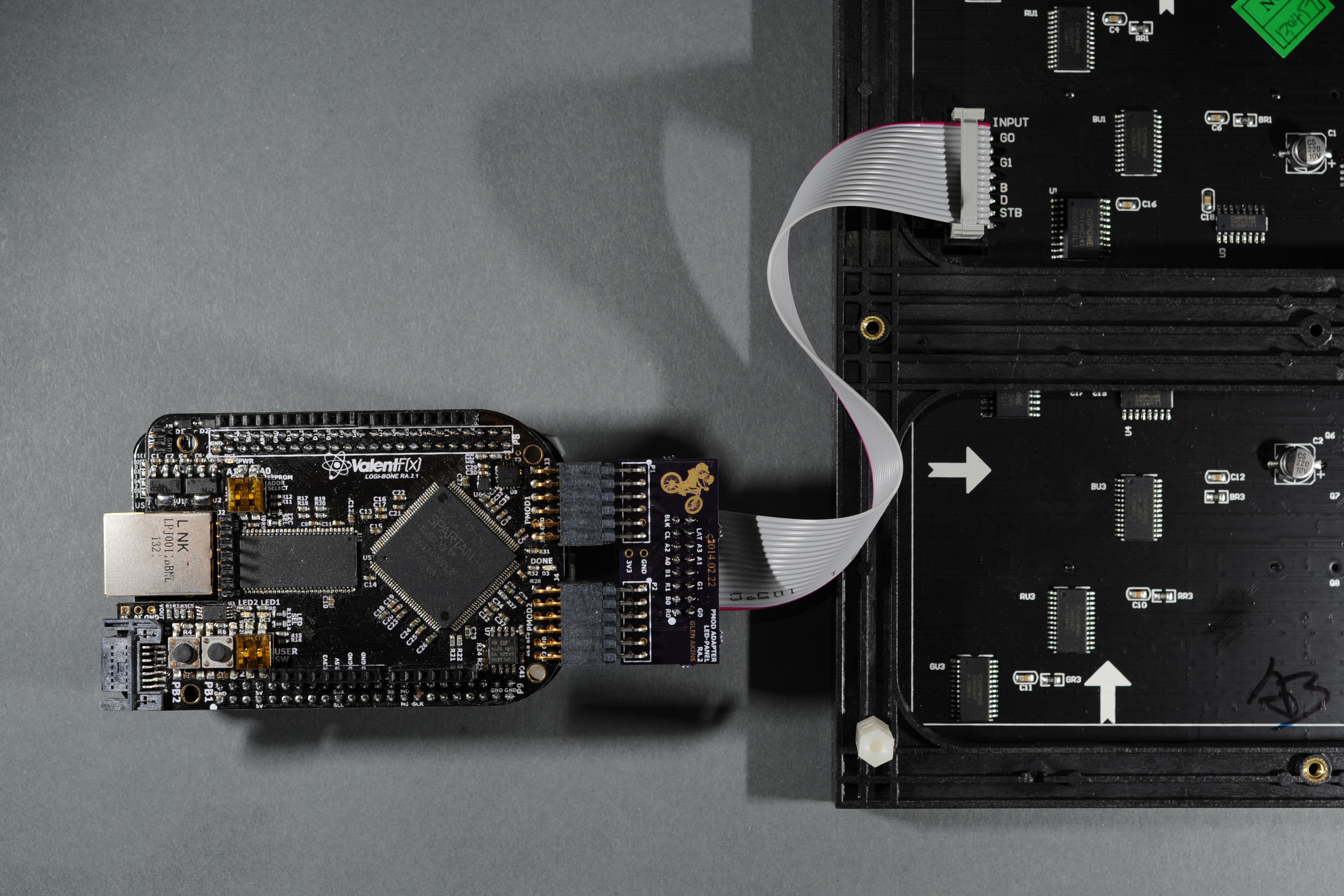
Figure 13. LogiBone FPGA board connected to RGB LED panel using the PMOD-to-display adapter board.
Display Power Supply Connection
Once the data signals have been connected, make the power supply connection to the display. Figure 14 below shows the basics. Using the DC barrel jack adapter, connect the positive terminal of the power supply to the red wire of the wire harness and connect the negative terminal of the power supply to the black wire of the wire harness. Before connecting the wire harness to the display, use a volt meter to verify the polarity of the connections. Once you’ve verified the polarity, disconnect the power and plug the wire harness into the display.
I left the spade lugs on the wire harness because I plan on using the display in a bigger project and don’t want to remove them until I’m sure I don’t need them in the bigger project. If you leave the spade lugs on too, be careful they don’t accidentally short to any other electronics. You might want to wrap them with electrical tape just to be sure. If you don’t need or want the spade connectors, feel free to cut them off, strip a bit of insulation off the wires, and connect them directly to the DC barrel jack adapter.
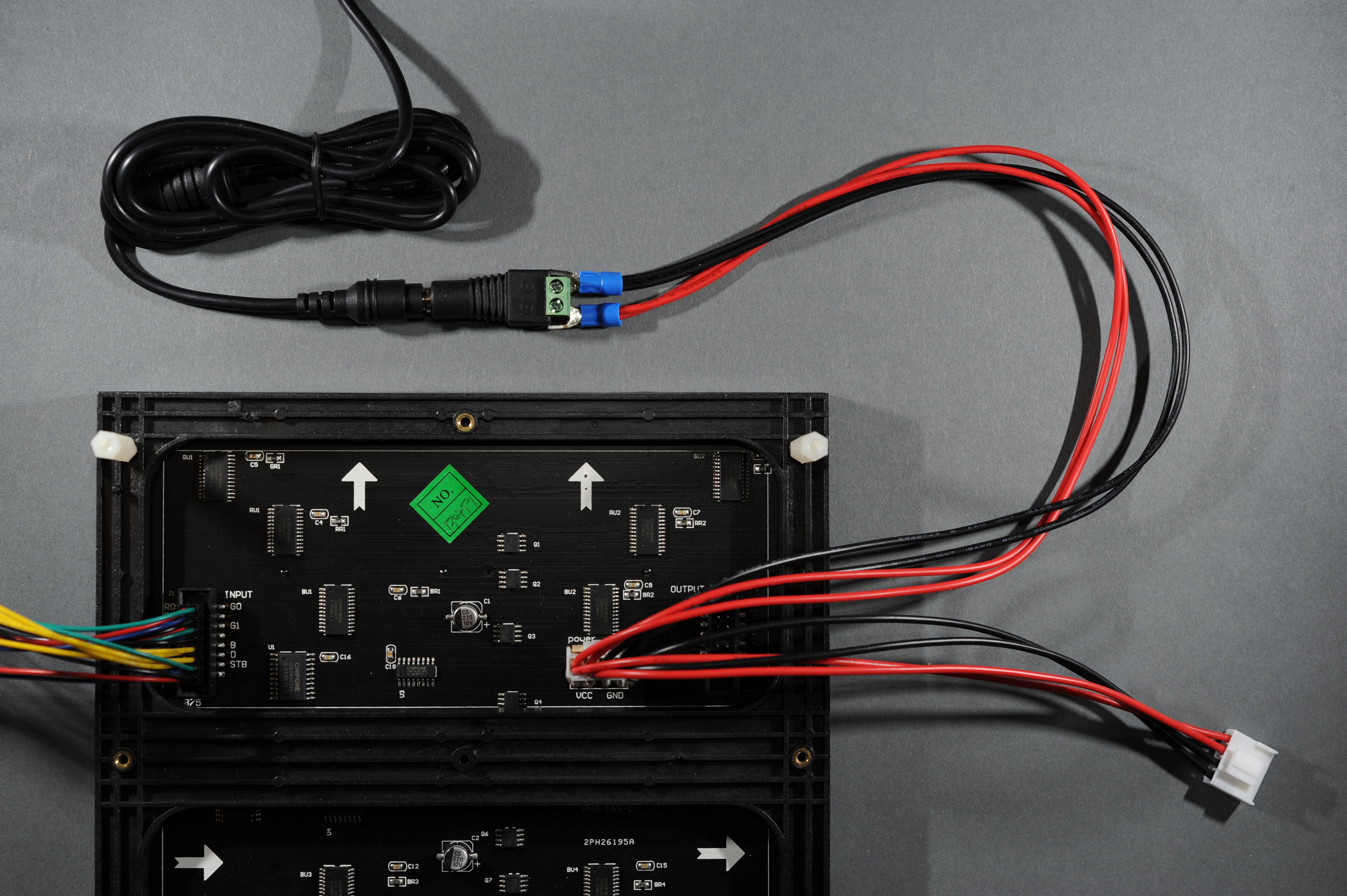
Figure 14. Connecting the power supply to the RGB LED panel using a female DC barrel jack adapter.
Downloading and Compiling the Software
The stock LogiBone Ubuntu image includes both the git revision control software and the GCC C/C++ compiler suite. We'll use git to clone the code repository to the BeagleBone Black then we’ll use g++, the GCC C++ compiler, to compile the C software to drive the panel.
Change to your home directory using the cd command and execute the git clone command to retrieve the repository:
ubuntu@arm:$ cd

ubuntu@arm:$ git clone http://github.com/bikerglen/beagle led-panel

Cloning into 'led-panel'...

remote: Reusing existing pack: 226, done.

remote: Total 226 (delta 0), reused 0 (delta 0)

Receiving objects: 100% (226/226), 61.51 KiB | 110 KiB/s, done.

Resolving deltas: 100% (84/84), done.


ubuntu@arm:$
The 'cd' command without any arguments changes to your home directory. The git clone command copies the repository from the specified URL to the 'led-panel' directory. If you want to use a different name for the directory, feel free but you'll need to change the path the in the rest of the commands that follow too.
Now change directories to the 'software' directory and execute the 'make' command to build the code:
ubuntu@arm:$ make
g++ -c runcircle.cpp
g++ -c pattern.cpp
g++ -c circle.cpp
g++ -o runcircle runcircle.o pattern.o circle.o
g++ -c runperlin.cpp
g++ -c perlin.cpp
g++ -o runperlin runperlin.o pattern.o perlin.o
g++ -c runwash.cpp
g++ -c wash.cpp
g++ -o runwash runwash.o pattern.o wash.o
g++ -c runtwinkle.cpp
g++ -c twinkle.cpp
g++ -o runtwinkle runtwinkle.o pattern.o twinkle.o
g++ -c runwipe.cpp
g++ -c wipe.cpp
g++ -o runwipe runwipe.o pattern.o wipe.o
g++ -o blank blank.cpp
g++ -o picture picture.cpp
Congratulations! All the code is now compiled. This builds the runcircle, runperlin, runwash, runtwinkle, runwipe, blank, and picture commands. Each of the 'run' commands produces a different animated pattern on the display. The blank command clears the display. The picture command displays an image on the panel. The filename of the image is supplied as the first argument to the command. The image must be a 32x32 24-bit color image in interleaved RGB format.
Running the Panel Using the Stock Bit File
Now let’s run the panel. We have two preparation steps to perform then we can run our first animated pattern on the display. The first preparation step is to configure the BeagleBone Black hardware to use the LogiBone FPGA board. Once that’s done, we need to load the FPGA’s configuration file into the FPGA.
Device Tree Configuration
The BeagleBone Black Ubuntu distribution uses kernel device trees to configure the CPU to use any attached capes or other hardware. The device tree maps hardware functions to pins, sets the data direction registers for pins, and configures any other registers in the CPU needed to use the attached hardware. Once the device tree for the added hardware has been loaded, the linux kernel loadable modules for the attached hardware’s device drivers can be loaded into the kernel. The stock LogiBone Ubuntu image includes a shell script to configure the device tree for the LogiBone FPGA board and load the LogiBone board’s hardware driver kernel modules.
Another function of the device tree is to configure the timing of the GPMC bus. SInce we modified the timing of the GPMC bus in our RTL, we need to make a few changes to the default device tree configuration file for the LogiBone FPGA board so that the CPU implements the same modified timng. The device tree file containing this modified timing is called “BB-BONE-LOGIBONE-SLOW.dts’ and is in the repository we cloned to our BBB early. There’s also a shell script called ‘setup_device-tree-slow.sh’ that compiles the .dts file into a .dtbo file, loads the modified device tree configuration file, and loads the LogiBone FPGA board’s device driver. We need to copy both the dts file and the shell script to our home directory:
ubuntu@arm:$ cd

ubuntu@arm:$ cp led-panel/projects/led-panel-v01/config-scripts/setup_device-tree-slow.sh .

ubuntu@arm:$ cp led-panel/projects/led-panel-v01/config-scripts/BB-BONE-LOGIBONE-SLOW.dts .


ubuntu@arm:$
Now that the shell script and device tree configuration file have been copied to the home directory, let’s run them:
ubuntu@arm:$ cd

ubuntu@arm:$ sudo ./setup_device-tree-slow.sh

rm: cannot remove `/lib/firmware/BB-BONE-LOGIBONE-SLOW.dtbo': No such file or directory

 0: 54:PF---

 1: 55:PF---

 2: 56:PF---

 3: 57:PF---

 7: ff:P-O-L Override Board Name,SLOW,Override Manuf,BB-BONE-LOGIBONE


ubuntu@arm:$
The first time the shell script is executed, the .dtbo file does not exist so you’ll get an error message that you can safely ignore. Also note that you may be prompted to enter your user password in order to authenticate yourself to the sudo command and run the setup shell script as root.
The device tree is now configured and the LogiBone board’s kernel level device driver has been loaded! Time to configure the FPGA.
FPGA Configuration
The next step is to load the configuration bit file into the FPGA. The configuration bit file is generated by the Xilinx ISE tools and contains our complete synthesized and routed design. Without the configuration file, the FPGA is nothing but a bunch of disconnected gates, memories, lookup tables, and routing resources. The configuration file connects the various resources together in the FPGA in such a way as to implement the logic we specified in our source code. The process of turning the source code into elements that exist in the FPGA is called synthesis. Xilinx divides the synthesis process into two stages: translation, where the code is compiled into primitive gates, and mapping, where the gates are arranged into CLBs and LUTs. The process of determining exactly which elements in the FPGA are used and how they’re connected using the available gates and routing resources is called place and route. After synthesis and place and route, a third process called static timing analysis runs to ensure that the design operates at the requested speed.
The LogiBone board’s stock Ubuntu image includes a utility called logi_loader in /usr/local/bin. The logi_loader utility loads a bit file specifed on the command line into the FPGA. The repository cloned onto the BBB earlier contains a pre-built configuration bit file so we can get started quickly with the FPGA and the display. Let’s give our FPGA some intelligence by loading the pre-built bit file into it using the logi_loader command:
ubuntu@arm:$ cd

ubuntu@arm:$ sudo logi_loader led-panel/projects/led-panel-v01/fpga/bitfiles/beagle01.bit

0+1 records in

0+1 records out

340714 bytes (341 kB) copied, 0.963579 s, 354 kB/s


ubuntu@arm:$
If all is well, the two user LEDs on the LogiBone FPGA should be blinking at slightly different rates. At this point you can connect power to the display. The display should be blank. (During the FPGA design phase, I set the defaults contents of the memories in the design to be all zero. A welcome message would have been cool too.)
Running a Pattern
Now let’s run one of the patterns we compiled earlier on the display. The Perlin noise pattern is pretty cool. Change to the software directory and run the runperlin executable as root:
ubuntu@arm:$ cd

ubuntu@arm:$ cd led-panel/projects/led-panel-v01/software/

ubuntu@arm:$ sudo ./runperlin


^Cubuntu@arm:$
Hopefully, the display is showing a mesmerizing and constantly changing pseudorandom pattern now! If not, make sure you included sudo in front of ./runperlin to run the command as root. The /dev/logibone_mem devce is only accessible by root. If the colors seem odd, check that the signals to the column drivers are connected correctly. If rows are swapped, check the signals to the row drivers. If the display looks like the top and bottom are swapped, check that R0,G0,B0 are not swapped with R1,G1,B1. If that fails, use a logic analyzer or scope to examine the signals between the display and the FPGA and ensure they look like their counter parts in the simulation of the FPGA.
Once you have everything working and have had enough of the Perlin noise, type ctrl-c to exit the runperlin program. Experiment with running some of the other patterns. The runwash and runcircle animations are pretty cool. There are also a biker and a beagle raw image files for use with the picture command in the repository. If you have the display sitting between you and your monitor and it’s starting to burn your eyes, use the blank command to clear the display back to all black.
Modifying an Existing Pattern
Let’s make a quick change to the Perlin noise display, compile the change, and re-run the runperlin command. The Perlin noise algorithm has an x/y scale parameter that controls the rough size of the displayed blobs. Let’s change this from 8 / 64 to 4 / 64 and observe the effects on the displayed images.
The Perlin subclass is declared in perlin.h. Open perlin.h using an editor (like vi) on the BBB and look for the longer of the two C++constructors:
        // constructor

        // m_hue_option is hue offset from 0.0 to 1.0 for mode 1, hue step for modes 2 and 3

        Perlin (const int32_t width, const int32_t height,

            const int32_t mode, const float xy_scale,


            const
 float z_step, const float z_depth, const float hue_options);
As you can see above, the fourth argument to the constructor is xy_scale and it is of type float. That is the parameter we want to change.
runperlin.cpp declares gPattern of type Perlin and then instantiates an instance of that class using the new operator. Find the “gPattern = new Perlin (…);” in runperlin.cpp:
    // create a new pattern object -- perlin noise, mode 2 long repeating

    gPattern = new Perlin (DISPLAY_WIDTH, DISPLAY_HEIGHT, 2, 8.0/64.0, 0.0125, 512.0, 0.005);
The fourth argument to the constructor is 8.0/64.0. Let’s change that to 4.0/64.0:
    // create a new pattern object -- perlin noise, mode 2 long repeating

    gPattern = new Perlin (DISPLAY_WIDTH, DISPLAY_HEIGHT, 2, 4.0/64.0, 0.0125, 512.0, 0.005);
Save the file and exit the editor. Now recompile everything and run the runperlin command again as root:
ubuntu@arm:$ make

g++ -c runperlin.cpp

g++ -o runperlin runperlin.o pattern.o perlin.o

ubuntu@arm:$ sudo ./runperlin


ubuntu@arm:$
Notice the different size of the blobs compared to the first time you executed the runperlin command?
Extra credit: Make the runperlin script listen for UDP packets containing new xy_scale and z_step parameters and change those parameters using the setter functions of the Perlin class as new UDP packets arrive. Use an Arduino, an Ethernet shield, and two potentiometers to generate the UDP packets.
Rebuilding the Bit File
If you would like to edit the led panel Verilog to include your own modifications, you’ll eventually need to rebuild the FPGA and create a new configuration bit file. Let’s walk through the process of rebuilding the FPGA from the original source code. You can then modify the source code to include your own changes and run it through the process in a similar manner. Note that rebuilding the FPGA and configuraiton bit file requires that the Xilinx ISE WebPack tools are installed.
The first step is to copy the ~/led-panel/beagle/projects/led-panel-v01/fpga directory from the BeagleBone Black to the machine where the Xilinx ISE tools are installed. This directory contains the Verilog source code for driving the LED panel, the Xiliinx ISE project files, and the Xilinx IP core generator files for the PLL and memories. You can perform the copy in one of several ways. You can clone the repostiory from GitHub down to your build machine, use scp to copy the directory from the BeagleBone Black to the build machine, or use an FTP client such as Filezilla (using port 22 for SFTP) to copy the directories from the BeagleBone Black to the build machine. The first two solutions work well if your build machine is running Linux. I'd suggest using Filezilla if your build machine is running Windows.
Once the directory is copied, launch the Xiinx ISE Project Navigator from the Windows start menu as shown below in Figure 15. On Linux, ensure the path to the tools is in your path environment variable and execute ise from the command line.
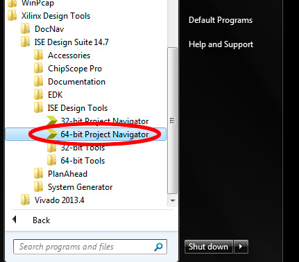
Figure 15. Launching the Xilinx ISE Project Navigator
Once the tool has launched, close any projects that opened when the the tool launched using the File menu then the Close Project option. Now click the “Open Project…” button as shown below in Figure 16.
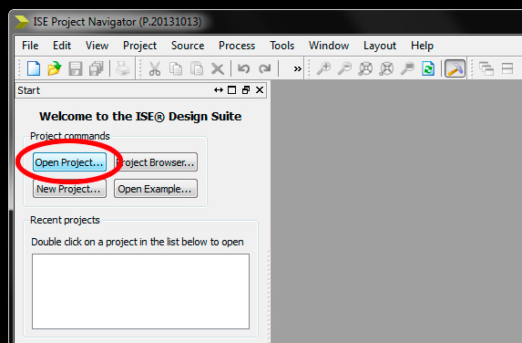
Figure 16. Open project button when no other projects are opened.
The ISE GUI will display a standard file chooser dialog bog as shown below in Figure 17. Navigate to the build directory inside the fpga directory you copied to the build machine earlier. Select the beagle01.xise project file from this directory and click open.
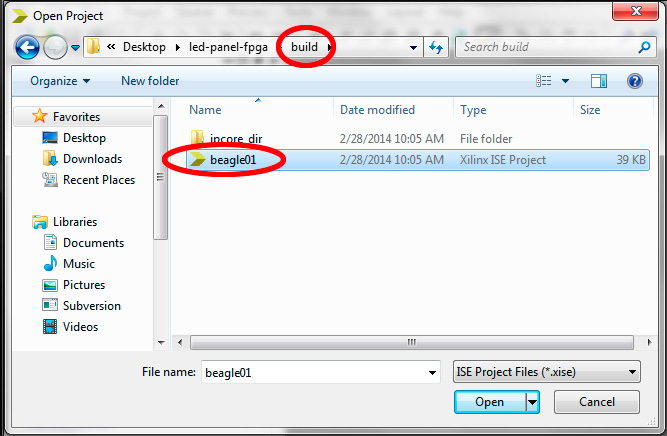
Figure 17. Opening the beagle01.xise project file.
The tool will open the beagle01 project and do some initial processing on the design. If the tool cannot find any files in the design, it will alert you to the missing files and give you the opportunity to locate those files now. Once everything has opened successfully, the screen will look similar to that in Figure 18. To rebuild the design from the original Verilog, click Implementation and click beagle01 in the hierarchy pane. Finally right click Generate Programming File and select Rerun All. These sections of the screen are highlighted in red in Figure 18 below.
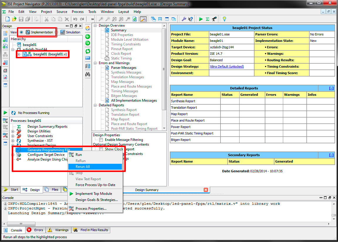
Figure 18. Project successfully opened with items required to rebuild entire design highlighted.
Once you click Rerun All, the tool will re-run the entire flow, starting from the source code, through synthesis, translation, mapping, place and route, and static timing analysis. If all of these processes run successfully, the tool will generate a programming file called beagle01.bit in the build directory. After generating the programming file successfully, the screen will look something like Figure 19.
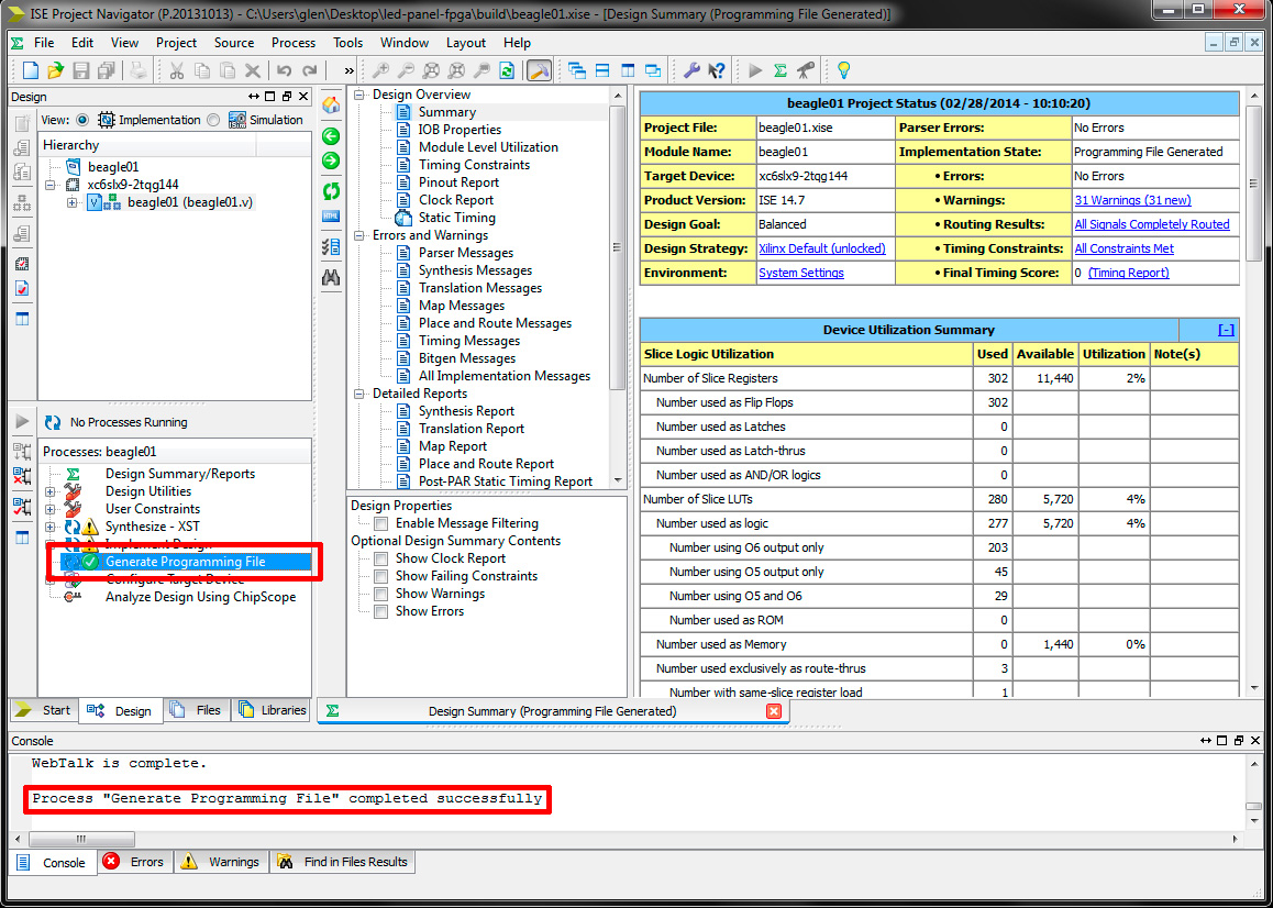
Figure 19. Successful synthesis, mapping, translation, place and route, and programming file generation.
Once the bit file has been generated, the bit file can be copied back to the BeagleBone Black using scp or an FTP client such as Filezilla (again use port 22 for SFTP). Once on the BeagleBone Black, the design can be loaded into the FPGA and tested using the logi_loader command.
Simulating the Design
With an FPGA, the tempation is there to develop your RTL just like you do any old piece of code: write, compile, debug, and iterate. That does not work for FPGA development. First, synthesis and place and route, especially on larger designs, can take much longer than compiling C or C++ code. Second, it’s really hard to observe signals inside an FPGA running in a real system.
Simulation solves both of these problems. Simulation speeds the time between write, compile, and debug iterations by replacing the lengthy synthesis / routing processes with what can be a much briefer compile, elaborate, and run process. Simulation also lets you observe every signal of interest in the FPGA at once. I cannot emphasize it enough. The key to creating a working FPGA is having a working simulation. The keys to having a working simulation are to accurately model the hardware attached to the FPGA and to target the simulation to the specific behaviors you want to observe in the FPGA. And a lot of time, the behaviors you want to observe are not only the normal operational behavior of the system but also the behavior of the system in response to error conditions.
Simulations require a testbench. The testbench contains instantiations of any device models (models of any hardware outside the FPGA), an instantiation of the device under test (the RTL for the FPGA), and test stimulus (for example, a test script used to run a series of steps in a test plan against the FPGA RTL). Additionally, the testbench may contain clock generators to generate the clocks used by the system and scripts to automate checking the results of the simulation.
Our testbench module is called testbench and is in the file testbench.v inside the fpga/test directory. In our testbench, we have a model of the GPMC host running inside the CPU on the BeagleBone Black, an instance of the beagle01 top-level module for our FPGA, a clock generator, a test script that writes data into the FPGA using the GPMC bus, and some code to monitor the column outputs from the FPGA,
Let’s run a quick simulation of the LED panel FPGA using the isim simulator built into the Xilinx ISE WebPack software and our testbench. Launch the Xilinx ISE Project Navigator and open the beagle01.xise project. Once the project is open, click Simulation and click on testbench (testbench.v) in the Hierarchy panel. Expand the ISim Simulator process, right click on Simulate Behavioral Model and select Rerun All. These sections of the screen are highlighted in red in Figure 20 below.

Figure 20. Launching ISim.
Once Rerun All is selected, the ISim simulator will launch. The source code for the testbench, the models, the FPGA, and any Xilinx IP core generator modules will be compiled and elaborated. Once elaborated, the simulation will begin running. Our testbench uses the $finish system task to stop the simulator once the test has completed. Once the simulation has run to completion, the screen will look like that in Figure 21 showing the line of code containing the $finish system task that caused the simulation to stop. Click the little X highlighted by the red box in the Figure 21 to close the testbench.v file.
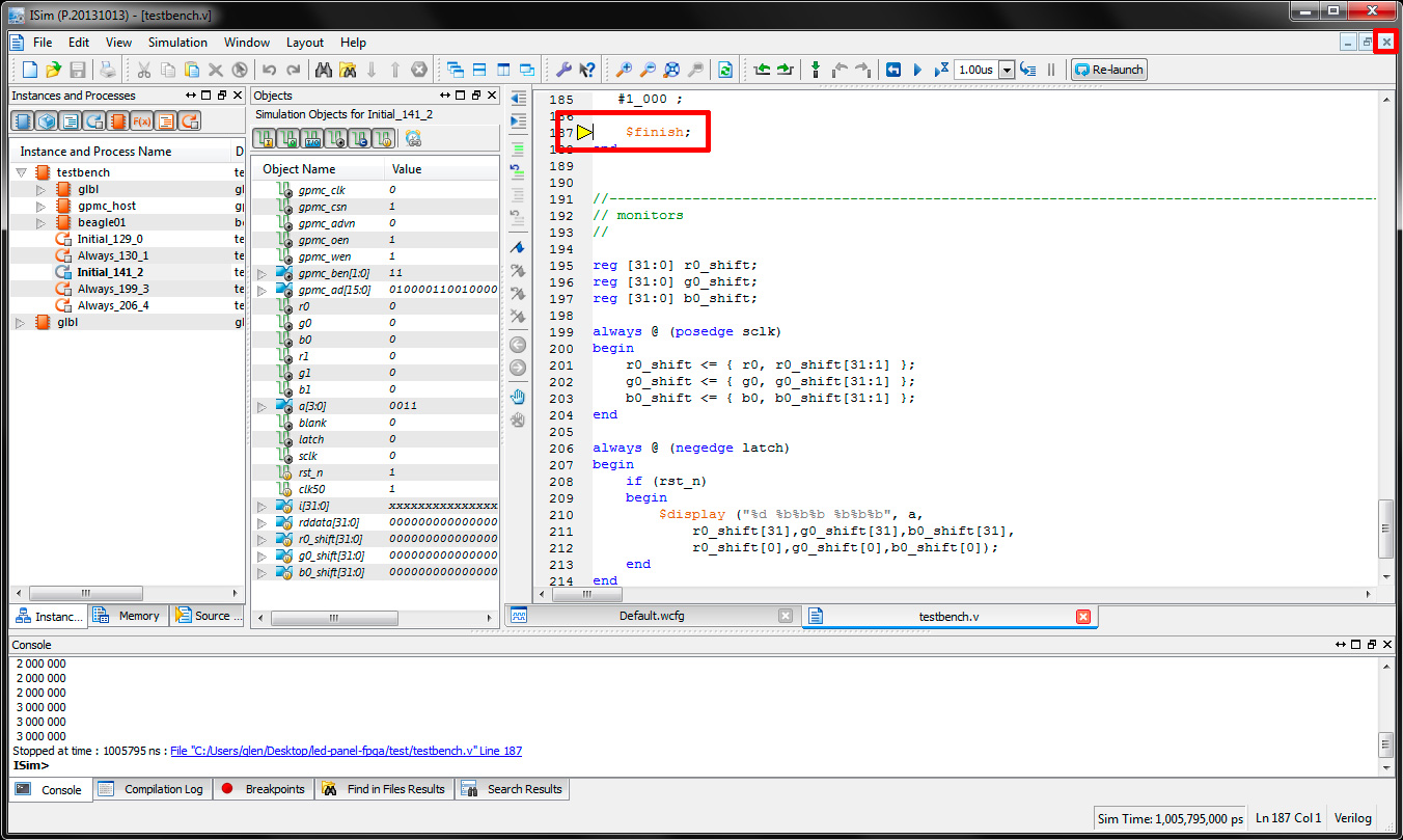
Figure 21. Simulation complete. Close the text editor to view the waveforms.
Once the testbench source code window is closed, the screen will show some waveforms for the simulation as shown below in Figure 22.
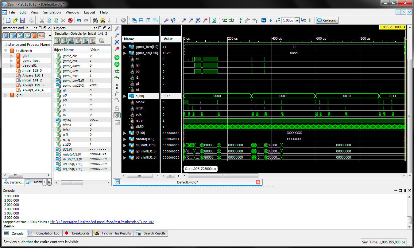
Figure 22. Simulation waveforms.
At this point you can use the mouse and menu items to zoom into and out of the waveforms. You can also dig into the hierachy of the testbench and the design using the left pane and add signals to the waveform display by dragging signals from the middle pane to the waveform display on the right side of the window. To update the waveforms to contain values for the newly added signals, re-run the simulation using the Rerun item under the Simulation menu. If you modified the test bench or the FPGA source code, you’ll need to relaunch the simulator using the Relaunch item under the Simulation menu. Relaunch will recompile and re-elaborate the testbench, modules, and cores in the design. Be sure to save the wcfg file if you want to have the same signals displayed in the waveforms pane after the simulator has relaunched.
Creating a New Pattern Subclass
To create a new class to display a new pattern on the panel, derive a subclass from the parent Pattern class. Listings 1 and 2 below show the minimum contents of the header and C++ source files for a new pattern subclass called MyPattern.
#ifndef __mypattern_h_
#define __mypattern_h_
class MyPattern : public Pattern

{

    public:
        // constructor

        MyPattern (const int32_t width, const int32_t height);
        // destructor

        ~MyPattern (void);
        // reset to first frame in animation

        void init (void);
        // calculate next frame in the animation

        bool next (void);
private:
        // any private control, configuration, state variables, etc.

};
#endifListing 1. Example pattern subclass C++ header file.
#include <stdio.h>
#include <stdlib.h>

#include <stdint.h>
#include "globals.h"

#include "pattern.h"

#include "mypattern.h"
//---------------------------------------------------------------------------------------------

// constructors

//
MyPattern::MyPattern (const int32_t width, const int32_t height) : Pattern (width, height)

{

}
//---------------------------------------------------------------------------------------------

// destructor

//
MyPattern::~MyPattern (void)

{

}
//---------------------------------------------------------------------------------------------

// init -- reset to first frame in animation

//
void MyPattern::init (void)

{

    // code to reset to first frame in animation

}
//---------------------------------------------------------------------------------------------

// next -- calculate next frame in animation

//
bool MyPattern::next (void)

{

    // code to generate next frame in animation
}Listing 2. Example pattern subclass C++ source file.
Becase the init and next methods are defined as pure virtual functions in the parent Pattern class, your new subclass must define the init and next methods.
The init method must contain code to reset the animation to the first frame of the animation. If you were creating a Pattern subclass to display an animated GIF on the LED panel, your init method, might open the GIF file, parse the frames in the file, store those frames in local memory, set the frame pointer to the first frame of the GIF, and set the frame delay timer to 0. The init method should not modify gLevels or call WriteLevels.
The next method must contain code to generate a frame of the animation, store the created frame in gLevels, and advance to the next frame of the animation. In our example subclass to display an animated GIF, when the frame delay timer expires, we’d copy the frame of the animation pointed to by the frame pointer to the gLevels buffer, advance the frame pointer to the next frame, and set the frame delay timer to the delay between frames of the GIF animation. If the timer had not expired, we’d decrement the timer and return without doing anything else.
The next method returns a boolean value to indicate when a convenient stopping point in the animation has been reached. In the GIF example, the next method might usually return false but would return true after the last frame of the animated GIF has been displayed for the amount of time indicated by the frame delay timer. This boolean value indicates to the calling function that now would be a good time to either increment a count of how many times the animation has been displayed or that it is a good time to switch to displaying a different pattern or animation. The next method should not call WriteLevels; only the caller of next should call WriteLevels.
After coding your new pattern subclass, you’ll need to add a few lines to the Makefile to compile the pattern subclass. You’ll also need to copy, modify, and compile one of the run<pattern>.cpp source code files to instantiate and run the pattern.
Extra credit: create a program to display mulitple patterns in a sequence. The patterns should change after each animation has run for one complete cycle. Use the the return value of the next method of each pattern subclass to determine when an animation sequence has completed.
Ideas for Improvement
The following are some ideas for improving the project.
- Implement global dimming.
- Use the GPMC bus in synchronous mode.
- Reduce the number of clocks required to shift the column data bits to two clocks. This requires learning which edge of SCLK latches the data on R0, G0, B0, R1, G1, B1.
- Drive more panels. Requires running at > 10MHz and optimizing the SCLK shift process down to two clocks.
References
The following references were used during construction of this project.
Adafruit’s RGB LED Panel Library on GitHub
Ken Perlin’s Original Perline Noise Source Code
Casey Duncan’s Python Noise Library on GitHub
Matt Zucker’s Perlin Noise Math and Seamless Tiling FAQ
Cliff Cummings’ Paper on Clock Domain Crossing Design and Verification Techniques
LED Dimming Using Binary Code Modulation
Afterword
I eventually created a new version of the project to drive six panels. Files related to the “6up” version of the project can be found in the /beagle/projects/led-panel-6up directory of my github repository. Unlike the “v01” project in the github repository and described in this tutorial, the “6up” project is not 100% ready-to-run out of the box. For example, there’s no step-by-step guide, you’ll need to build your own bitfile, and you’ll need to compile the software. The new Verilog does, however, includes global dimming support, uses only two clocks per 6 bits of RGB data to shift data into the panels, and supports up to six panels daisy chained together.
Here are a few photos of some of the projects built using the “6up” version of the project:
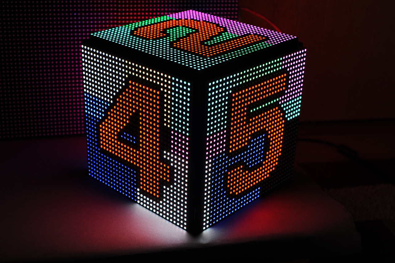
Figure 23. Five-sided cube built with five panels and the “6up” Verilog.

Figure 24. Six-panel wall front.

Figure 25. Six-panel wall rear.
Mountain bike season is once again upon us. Time to go ride!